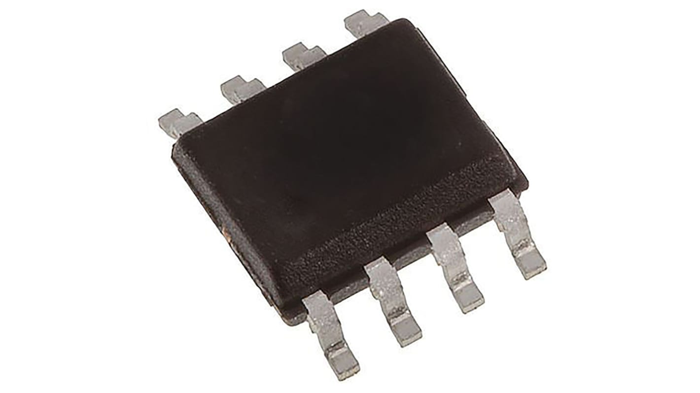
Infineon Isolated HEXFET 2 Type P, Type N-Channel MOSFET, 3.5 A, 30 V Enhancement, 8-Pin SOIC IRF9952TRPBF
- RS庫存編號:
- 827-3934
- 製造零件編號:
- IRF9952TRPBF
- 製造商:
- Infineon

此圖片僅供參考,請參閲產品詳細資訊及規格
可享批量折扣
小計(1 包,共 20 件)*
TWD418.00
(不含稅)
TWD438.80
(含稅)
訂單超過 $1,300.00 免費送貨
有庫存
- 340 件準備從其他地點送貨
- 加上 3,620 件從 2026年5月22日 起發貨
**需要更多嗎?**輸入您需要的數量,然後按一下「查看送貨日期」以查詢更多庫存和送貨詳細資訊。
單位 | 每單位 | 每包* |
|---|---|---|
| 20 - 980 | TWD20.90 | TWD418.00 |
| 1000 + | TWD20.30 | TWD406.00 |
* 參考價格
- RS庫存編號:
- 827-3934
- 製造零件編號:
- IRF9952TRPBF
- 製造商:
- Infineon
規格
產品概覽和技術數據資料表
法例與合規
產品詳細資訊
透過選取一個或多個屬性來查找類似產品。
選取全部 | 屬性 | 值 |
|---|---|---|
| 品牌 | Infineon | |
| Channel Type | Type P, Type N | |
| Product Type | MOSFET | |
| Maximum Continuous Drain Current Id | 3.5A | |
| Maximum Drain Source Voltage Vds | 30V | |
| Series | HEXFET | |
| Package Type | SOIC | |
| Mount Type | Surface | |
| Pin Count | 8 | |
| Maximum Drain Source Resistance Rds | 400mΩ | |
| Channel Mode | Enhancement | |
| Minimum Operating Temperature | -55°C | |
| Typical Gate Charge Qg @ Vgs | 6.1nC | |
| Maximum Power Dissipation Pd | 2W | |
| Forward Voltage Vf | 0.82V | |
| Transistor Configuration | Isolated | |
| Maximum Operating Temperature | 150°C | |
| Length | 5mm | |
| Height | 1.5mm | |
| Standards/Approvals | No | |
| Number of Elements per Chip | 2 | |
| Automotive Standard | No | |
| 選取全部 | ||
|---|---|---|
品牌 Infineon | ||
Channel Type Type P, Type N | ||
Product Type MOSFET | ||
Maximum Continuous Drain Current Id 3.5A | ||
Maximum Drain Source Voltage Vds 30V | ||
Series HEXFET | ||
Package Type SOIC | ||
Mount Type Surface | ||
Pin Count 8 | ||
Maximum Drain Source Resistance Rds 400mΩ | ||
Channel Mode Enhancement | ||
Minimum Operating Temperature -55°C | ||
Typical Gate Charge Qg @ Vgs 6.1nC | ||
Maximum Power Dissipation Pd 2W | ||
Forward Voltage Vf 0.82V | ||
Transistor Configuration Isolated | ||
Maximum Operating Temperature 150°C | ||
Length 5mm | ||
Height 1.5mm | ||
Standards/Approvals No | ||
Number of Elements per Chip 2 | ||
Automotive Standard No | ||
Infineon HEXFET Series MOSFET, 2.3A/3.5A Maximum Continuous Drain Current, 2W Maximum Power Dissipation - IRF9952TRPBF
This versatile MOSFET delivers high performance in a Compact package, integrating both N-channel and P-channel configurations. It is designed for effective operation in various electronic applications, ensuring efficiency and dependability. With a maximum drain current of 3.5A and a maximum drain-source voltage of 30V, it is suitable for applications that require robust switching capabilities.
Features & Benefits
• Dual-channel configuration enhances design flexibility
• Surface mount design simplifies PCB assembly
• Low resistance (150mΩ and 400mΩ) reduces power loss
• High temperature operation (+150°C) ensures reliability in extreme conditions
• Improved gate charge characteristics enhance switching efficiency
• Isolated transistor configuration minimises cross-talk for cleaner signals
Applications
• Power management solutions
• Electric vehicle systems for improved efficiency
• Industrial automation and control
• Renewable energy systems for optimal performance
• Consumer electronics for enhanced device performance
How does the isolation of this device benefit my application?
The isolated configuration minimises interference among circuits, ensuring clean signals and preventing unwanted interactions between components.
What temperature range can this device handle during operation?
It can operate within a temperature range of -55°C to +150°C, making it suitable for extreme conditions.
Can I use this product in my surface mount PCB design?
Yes, its surface mount design allows for easy integration into PCB layouts, optimising space and enhancing thermal performance.
What factors should I consider when using this for switching applications?
Ensure the maximum gate-source voltage of ±20V is not exceeded and verify that the gate charge aligns with your switching frequency for optimal performance.
How do the specifications affect my power efficiency?
With low on-resistance and high continuous drain current, this MOSFET contributes to minimal power loss, enhancing overall energy efficiency in your circuit designs.
相關連結
- Infineon Isolated HEXFET 2 Type P 3.5 A 8-Pin SOIC
- Infineon Isolated HEXFET 2 Type P 3.5 A 8-Pin SOIC
- Infineon Isolated HEXFET 2 Type P 3.5 A 8-Pin SOIC IRF7105TRPBF
- Infineon Isolated HEXFET 2 Type P-Channel MOSFET 55 V Enhancement, 8-Pin SOIC
- Infineon Isolated HEXFET 2 Type P-Channel MOSFET 20 V Enhancement, 8-Pin SOIC
- Infineon Isolated HEXFET 2 Type P-Channel MOSFET 30 V Enhancement, 8-Pin SOIC
- Infineon Isolated HEXFET 2 Type N 4 A 8-Pin SOIC
- Infineon Isolated HEXFET 2 Type P 7.3 A 8-Pin SOIC
