Vishay SIHK Type N-Channel MOSFET, 30 A, 650 V Enhancement, 8-Pin PowerPAK 10 x 12 SIHK085N60EF-T1GE3
- RS庫存編號:
- 268-8306
- 製造零件編號:
- SIHK085N60EF-T1GE3
- 製造商:
- Vishay

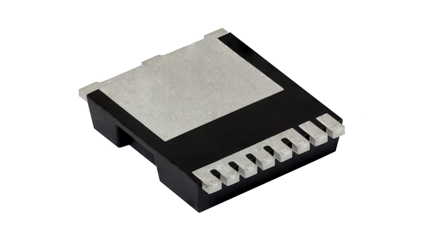
此圖片僅供參考,請參閲產品詳細資訊及規格
小計(1 卷,共 2000 件)*
TWD313,400.00
(不含稅)
TWD329,080.00
(含稅)
庫存資訊目前無法存取 - 請稍後再回來查看
單位 | 每單位 | 每卷* |
|---|---|---|
| 2000 + | TWD156.70 | TWD313,400.00 |
* 參考價格
- RS庫存編號:
- 268-8306
- 製造零件編號:
- SIHK085N60EF-T1GE3
- 製造商:
- Vishay
規格
產品概覽和技術數據資料表
法例與合規
產品詳細資訊
透過選取一個或多個屬性來查找類似產品。
選取全部 | 屬性 | 值 |
|---|---|---|
| 品牌 | Vishay | |
| Channel Type | Type N | |
| Product Type | MOSFET | |
| Maximum Continuous Drain Current Id | 30A | |
| Maximum Drain Source Voltage Vds | 650V | |
| Package Type | PowerPAK 10 x 12 | |
| Series | SIHK | |
| Mount Type | PCB | |
| Pin Count | 8 | |
| Maximum Drain Source Resistance Rds | 0.085Ω | |
| Channel Mode | Enhancement | |
| Minimum Operating Temperature | -55°C | |
| Forward Voltage Vf | 1.2V | |
| Maximum Power Dissipation Pd | 184W | |
| Typical Gate Charge Qg @ Vgs | 63nC | |
| Maximum Operating Temperature | 150°C | |
| Standards/Approvals | RoHS | |
| Length | 9.9mm | |
| Automotive Standard | No | |
| 選取全部 | ||
|---|---|---|
品牌 Vishay | ||
Channel Type Type N | ||
Product Type MOSFET | ||
Maximum Continuous Drain Current Id 30A | ||
Maximum Drain Source Voltage Vds 650V | ||
Package Type PowerPAK 10 x 12 | ||
Series SIHK | ||
Mount Type PCB | ||
Pin Count 8 | ||
Maximum Drain Source Resistance Rds 0.085Ω | ||
Channel Mode Enhancement | ||
Minimum Operating Temperature -55°C | ||
Forward Voltage Vf 1.2V | ||
Maximum Power Dissipation Pd 184W | ||
Typical Gate Charge Qg @ Vgs 63nC | ||
Maximum Operating Temperature 150°C | ||
Standards/Approvals RoHS | ||
Length 9.9mm | ||
Automotive Standard No | ||
- COO (Country of Origin):
- CN
Vishay SIHK Series MOSFET, 650V Maximum Drain Source Voltage, 30A Maximum Continuous Drain Current - SIHK085N60EF-T1GE3
This MOSFET is a high-voltage N-channel switching device designed for power conversion and control in industrial electronics. It operates as an enhancement-mode transistor suitable for PCB mounting and is intended for demanding applications that require robust thermal tolerance and substantial current handling.
Features and Benefits:
• 650V rating enables high-voltage switching capability • 30A continuous drain current supports heavy load duty • 0.085Ω Rds(on) reduces conduction losses at switching • 63nC typical gate charge allows predictable gate-drive design • 184W power dissipation permits significant heat throughput • 150°C maximum junction temperature supports high-temperature operation
Applications
• Suitable for high-voltage DC-DC converters in automation systems • Ideal for motor drive front-ends requiring high current headroom • Used for switch-mode power supplies in industrial electronics • Can be used for inverter stages in power control equipment
What gate-drive constraints should be considered for use?
The device tolerates gate voltages up to 30V and exhibits a typical total gate charge of 63nC, so drivers must supply sufficient charge and slew control within that voltage limit.
How should thermal management be arranged on the PCB?
With a maximum dissipation of 184W and high junction capability, provide substantial copper area, thermal vias and an appropriate heatsink attachment pattern to maintain safe operating temperatures.
What environmental temperature range will it tolerate during operation?
It operates down to -55°C and up to a maximum of 150°C, allowing deployment across broad ambient and elevated junction scenarios.
Which mounting approach is required for reliable assembly?
The part is intended for PCB mount in a PowerPAK 10x12 package with an 8-pin interface, so standard soldering processes for power packages should be used.
相關連結
- Vishay SIHK Type N-Channel MOSFET 650 V Enhancement, 8-Pin PowerPAK 10 x 12 SIHK085N60EF-T1GE3
- Vishay SIHK Type N-Channel MOSFET 650 V Enhancement, 8-Pin PowerPAK 10 x 12 SIHK105N60EF-T1GE3
- Vishay SIHK Type N-Channel MOSFET 650 V Enhancement, 8-Pin PowerPAK 10 x 12 SIHK045N60EF-T1GE3
- Vishay SIHK Type N-Channel MOSFET 650 V Enhancement, 8-Pin PowerPAK 10 x 12 SIHK125N60EF-T1GE3
- Vishay SIHK Type N-Channel MOSFET 650 V Enhancement, 8-Pin PowerPAK 10 x 12 SIHK185N60EF-T1GE3
- Vishay SIHK Type N-Channel MOSFET 600 V Enhancement, 8-Pin PowerPAK 10 x 12 SIHK155N60EF-T1GE3
- Vishay EF Type N-Channel MOSFET 650 V Enhancement, 4-Pin PowerPAK 8 x 8 SIHH125N60EF-T1GE3
- Vishay EF Type N-Channel MOSFET 650 V Enhancement, 4-Pin PowerPAK 8 x 8 SIHH186N60EF-T1GE3