Vishay EF Type N-Channel Power MOSFET, 6.5 A, 850 V Depletion, 3-Pin TO-220 SiHA17N80AEF-GE3
- RS庫存編號:
- 239-8622
- 製造零件編號:
- SiHA17N80AEF-GE3
- 製造商:
- Vishay

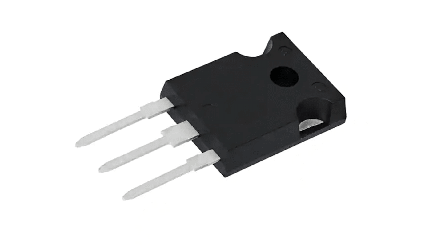
此圖片僅供參考,請參閲產品詳細資訊及規格
可享批量折扣
查看批量定價選項小計(1 包,共 2 件)*
TWD130.00
(不含稅)
TWD136.50
(含稅)
訂單超過 $1,300.00 免費送貨
有庫存
- 1,050 件準備從其他地點送貨
**需要更多嗎?**輸入您需要的數量,然後按一下「查看送貨日期」以查詢更多庫存和送貨詳細資訊。
單位 | 每單位 | 每包* |
|---|---|---|
| 2 - 8 | TWD65.00 | TWD130.00 |
| 10 - 18 | TWD64.00 | TWD128.00 |
| 20 - 24 | TWD63.00 | TWD126.00 |
| 26 - 98 | TWD61.00 | TWD122.00 |
| 100 + | TWD60.00 | TWD120.00 |
* 參考價格
- RS庫存編號:
- 239-8622
- 製造零件編號:
- SiHA17N80AEF-GE3
- 製造商:
- Vishay
規格
產品概覽和技術數據資料表
法例與合規
產品詳細資訊
透過選取一個或多個屬性來查找類似產品。
選取全部 | 屬性 | 值 |
|---|---|---|
| 品牌 | Vishay | |
| Channel Type | Type N | |
| Product Type | Power MOSFET | |
| Maximum Continuous Drain Current Id | 6.5A | |
| Maximum Drain Source Voltage Vds | 850V | |
| Package Type | TO-220 | |
| Series | EF | |
| Mount Type | Surface | |
| Pin Count | 3 | |
| Maximum Drain Source Resistance Rds | 0.305Ω | |
| Channel Mode | Depletion | |
| Maximum Power Dissipation Pd | 34W | |
| Maximum Gate Source Voltage Vgs | 30V | |
| Minimum Operating Temperature | -55°C | |
| Typical Gate Charge Qg @ Vgs | 63nC | |
| Forward Voltage Vf | 1.2V | |
| Maximum Operating Temperature | +150°C | |
| Standards/Approvals | RoHS | |
| Automotive Standard | AEC-Q101 | |
| 選取全部 | ||
|---|---|---|
品牌 Vishay | ||
Channel Type Type N | ||
Product Type Power MOSFET | ||
Maximum Continuous Drain Current Id 6.5A | ||
Maximum Drain Source Voltage Vds 850V | ||
Package Type TO-220 | ||
Series EF | ||
Mount Type Surface | ||
Pin Count 3 | ||
Maximum Drain Source Resistance Rds 0.305Ω | ||
Channel Mode Depletion | ||
Maximum Power Dissipation Pd 34W | ||
Maximum Gate Source Voltage Vgs 30V | ||
Minimum Operating Temperature -55°C | ||
Typical Gate Charge Qg @ Vgs 63nC | ||
Forward Voltage Vf 1.2V | ||
Maximum Operating Temperature +150°C | ||
Standards/Approvals RoHS | ||
Automotive Standard AEC-Q101 | ||
Vishay Series EF Power MOSFET, 850V Drain Source Voltage, 6.5A Drain Current - SiHA17N80AEF-GE3
This power MOSFET is a high-voltage switching transistor designed for demanding electrical and automotive contexts. It operates as an N-channel depletion device in a through-hole TO-220 surface package, providing a Compact solution for power conversion and control where robust voltage handling and thermal margin are required.
Features and Benefits:
• 850V maximum drain-source voltage for high-voltage applications • 6.5A continuous drain current enabling sustained load handling • 0.305 Ω Rds minimises conduction losses under load • 34W power dissipation supports elevated thermal budgets • 63 nC typical gate charge for predictable switching control • ±150 °C/-55 °C operating range offers wide temperature endurance
Applications
• Suitable for high-voltage DC-DC converter stages in industrial systems • Ideal for inverter front ends and power-factor circuits • Used for switch-mode power supplies in automation equipment • Can be used for automotive power electronics meeting AEC‑Q101 criteria • Used with gate drivers requiring defined charge characteristics
What gate-voltage limits should be observed during design?
The device tolerates gate excursion up to 30 V
designs should ensure gate‑drive circuits remain within this limit to prevent gate-oxide stress.
How should thermal management be implemented for reliable operation?
Given a 34W dissipation rating, attach an appropriate heatsink to the TO‑220 tab and ensure sufficient airflow to maintain junction temperatures within safe bounds.
What considerations apply to switching losses and driver selection?
With a typical gate charge of 63 nC, choose a driver capable of sourcing and sinking the required Peak currents to achieve the desired rise/fall times while managing switching losses.
Is the device suitable for automotive qualification processes?
It conforms to AEC‑Q101 standards for automotive MOSFETs, making it appropriate for designs that require automotive‑grade components.
What electrical polarity and channel behaviour should designers expect?
The transistor is an N‑channel depletion device, so circuit topology must account for its channel mode when implementing normally‑on or normally‑off switching arrangements.
相關連結
- Vishay EF Type N-Channel MOSFET 850 V Depletion, 3-Pin TO-220
- Vishay EF Type N-Channel MOSFET 850 V Depletion, 3-Pin TO-220 SIHA21N80AEF-GE3
- Vishay EF Type N-Channel MOSFET 850 V Depletion, 3-Pin TO-220 SIHA15N80AEF-GE3
- Vishay EF Type N-Channel MOSFET 850 V Depletion, 3-Pin TO-220
- Vishay EF Type N-Channel MOSFET 850 V Depletion, 3-Pin TO-220
- Vishay EF Type N-Channel MOSFET 650 V Depletion, 3-Pin TO-247 SIHG026N60EF-GE3
- Vishay EF Type N-Channel MOSFET 650 V Depletion, 3-Pin TO-263 SIHB055N60EF-GE3
- Vishay EF Type N-Channel MOSFET 650 V Depletion, 3-Pin TO-247