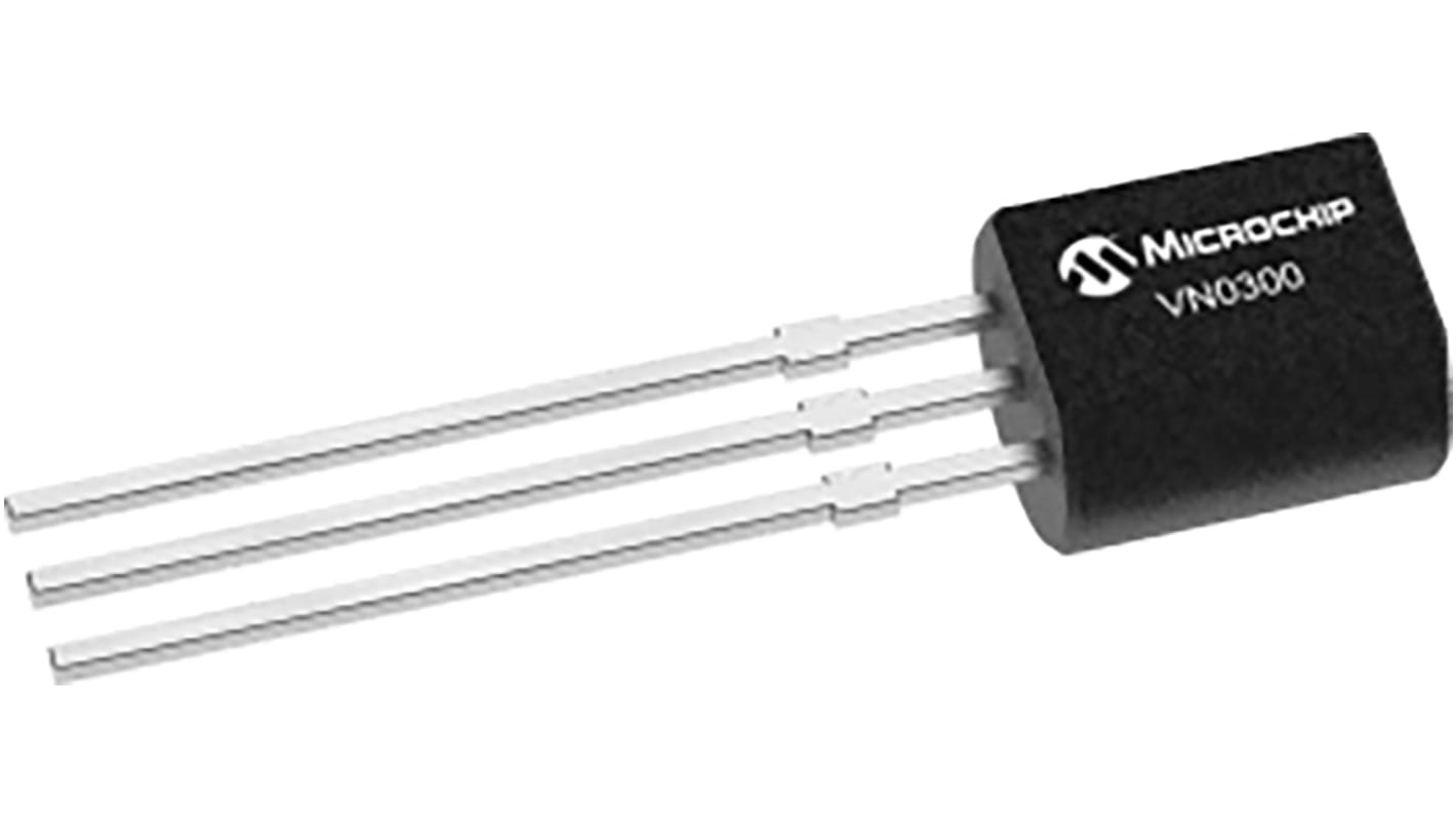
Microchip VN0300 Type N-Channel MOSFET, 640 mA, 30 V Enhancement, 3-Pin TO-92
- RS庫存編號:
- 177-9705
- 製造零件編號:
- VN0300L-G
- 製造商:
- Microchip

此圖片僅供參考,請參閲產品詳細資訊及規格
可享批量折扣
小計(1 袋,共 1000 件)*
TWD32,800.00
(不含稅)
TWD34,440.00
(含稅)
訂單超過 $1,300.00 免費送貨
暫時缺貨
- 從 2026年7月20日 發貨
**需要更多嗎?**輸入您需要的數量,然後按一下「查看送貨日期」以查詢更多庫存和送貨詳細資訊。
單位 | 每單位 | 每袋* |
|---|---|---|
| 1000 - 4000 | TWD32.80 | TWD32,800.00 |
| 5000 + | TWD29.50 | TWD29,500.00 |
* 參考價格
- RS庫存編號:
- 177-9705
- 製造零件編號:
- VN0300L-G
- 製造商:
- Microchip
規格
產品概覽和技術數據資料表
法例與合規
產品詳細資訊
透過選取一個或多個屬性來查找類似產品。
選取全部 | 屬性 | 值 |
|---|---|---|
| 品牌 | Microchip | |
| Channel Type | Type N | |
| Product Type | MOSFET | |
| Maximum Continuous Drain Current Id | 640mA | |
| Maximum Drain Source Voltage Vds | 30V | |
| Package Type | TO-92 | |
| Series | VN0300 | |
| Mount Type | Through Hole | |
| Pin Count | 3 | |
| Maximum Drain Source Resistance Rds | 3.3Ω | |
| Channel Mode | Enhancement | |
| Minimum Operating Temperature | -55°C | |
| Maximum Power Dissipation Pd | 1W | |
| Forward Voltage Vf | 0.9V | |
| Maximum Operating Temperature | 150°C | |
| Standards/Approvals | No | |
| Length | 5.08mm | |
| Height | 5.33mm | |
| Automotive Standard | No | |
| 選取全部 | ||
|---|---|---|
品牌 Microchip | ||
Channel Type Type N | ||
Product Type MOSFET | ||
Maximum Continuous Drain Current Id 640mA | ||
Maximum Drain Source Voltage Vds 30V | ||
Package Type TO-92 | ||
Series VN0300 | ||
Mount Type Through Hole | ||
Pin Count 3 | ||
Maximum Drain Source Resistance Rds 3.3Ω | ||
Channel Mode Enhancement | ||
Minimum Operating Temperature -55°C | ||
Maximum Power Dissipation Pd 1W | ||
Forward Voltage Vf 0.9V | ||
Maximum Operating Temperature 150°C | ||
Standards/Approvals No | ||
Length 5.08mm | ||
Height 5.33mm | ||
Automotive Standard No | ||
- COO (Country of Origin):
- TW
Microchip Technology MOSFET
The Microchip Technology through-hole mount N-channel MOSFET is a new age product with a drain-source voltage of 30V and a maximum gate-source voltage of 30V. It has drain-source resistance of 1.2ohms at a gate-source voltage of 10V. It has continuous drain current of 640mA and maximum power dissipation of 1W. The minimum and a maximum driving voltage for this MOSFET is 5V and 10V respectively. The MOSFET is an enhancement mode (normally off) MOSFET that utilizes a vertical DMOS structure and well-proven, silicon gate manufacturing process. This combination produces a device with the power handling capabilities of bipolar transistors and the high input impedance and positive temperature coefficient inherent in MOS devices. A significant characteristic of all MOS structures, this device is free from thermal runaway and thermally induced secondary breakdown. This vertical DMOS FET has been optimized for lower switching and conduction losses. The MOSFET offers excellent efficiency along with a long and productive life without compromising performance or functionality.
Features and Benefits
• Ease of paralleling
• Excellent thermal stability
• Free from secondary breakdown
• High input impedance and high gain
• Integral source drain diode
• Low CISS and fast switching speeds
• Low power drive requirement
• Operating temperature ranges between -55°C and 150°C
Applications
• Amplifiers
• Converters
• Drivers: relays, hammers, solenoids, lamps, memories, displays, bipolar transistors, etc.
• Motor controls
• Power supply circuits
• Switches
Certifications
• ANSI/ESD S20.20:2014
• BS EN 61340-5-1:2007
• JEDEC
相關連結
- Microchip VN0300 Type N-Channel MOSFET 30 V Enhancement, 3-Pin TO-92 VN0300L-G
- Microchip VP2206 Type P-Channel MOSFET -60 V Enhancement, 3-Pin TO-92
- Microchip VP2206 Type P-Channel MOSFET -60 V Enhancement, 3-Pin TO-92 VP2206N3-G
- Microchip Type N-Channel MOSFET 3-Pin TO-92
- Microchip Type N-Channel MOSFET 3-Pin TO-92 TP0606N3-G
- Microchip VN0104 Type N-Channel MOSFET 3-Pin TO-92 VN0104N3-G
- Microchip VN3205 Type N-Channel MOSFET 3-Pin TO-92 VN3205N3-G
- Microchip TN0604 Type N-Channel MOSFET 3-Pin TO-92 TN0604N3-G
