onsemi Dual PowerTrench 2 Type N-Channel MOSFET, 2.9 A, 30 V Enhancement, 6-Pin WDFN FDMA2002NZ
- RS庫存編號:
- 184-5019
- 製造零件編號:
- FDMA2002NZ
- 製造商:
- onsemi

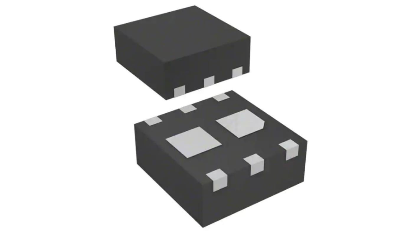
此圖片僅供參考,請參閲產品詳細資訊及規格
可享批量折扣
小計(1 包,共 20 件)*
TWD468.00
(不含稅)
TWD491.40
(含稅)
訂單超過 $1,300.00 免費送貨
有庫存
- 900 件準備從其他地點送貨
**需要更多嗎?**輸入您需要的數量,然後按一下「查看送貨日期」以查詢更多庫存和送貨詳細資訊。
單位 | 每單位 | 每包* |
|---|---|---|
| 20 - 740 | TWD23.40 | TWD468.00 |
| 760 - 1480 | TWD22.80 | TWD456.00 |
| 1500 + | TWD22.50 | TWD450.00 |
* 參考價格
- RS庫存編號:
- 184-5019
- 製造零件編號:
- FDMA2002NZ
- 製造商:
- onsemi
規格
產品概覽和技術數據資料表
法例與合規
產品詳細資訊
透過選取一個或多個屬性來查找類似產品。
選取全部 | 屬性 | 值 |
|---|---|---|
| 品牌 | onsemi | |
| Channel Type | Type N | |
| Product Type | MOSFET | |
| Maximum Continuous Drain Current Id | 2.9A | |
| Maximum Drain Source Voltage Vds | 30V | |
| Series | PowerTrench | |
| Package Type | WDFN | |
| Mount Type | Surface | |
| Pin Count | 6 | |
| Maximum Drain Source Resistance Rds | 268mΩ | |
| Channel Mode | Enhancement | |
| Minimum Operating Temperature | -55°C | |
| Typical Gate Charge Qg @ Vgs | 2.4nC | |
| Maximum Gate Source Voltage Vgs | 12 V | |
| Forward Voltage Vf | 0.9V | |
| Maximum Power Dissipation Pd | 1.5W | |
| Transistor Configuration | Dual | |
| Maximum Operating Temperature | 150°C | |
| Standards/Approvals | No | |
| Width | 2 mm | |
| Length | 2mm | |
| Height | 0.75mm | |
| Number of Elements per Chip | 2 | |
| Automotive Standard | No | |
| 選取全部 | ||
|---|---|---|
品牌 onsemi | ||
Channel Type Type N | ||
Product Type MOSFET | ||
Maximum Continuous Drain Current Id 2.9A | ||
Maximum Drain Source Voltage Vds 30V | ||
Series PowerTrench | ||
Package Type WDFN | ||
Mount Type Surface | ||
Pin Count 6 | ||
Maximum Drain Source Resistance Rds 268mΩ | ||
Channel Mode Enhancement | ||
Minimum Operating Temperature -55°C | ||
Typical Gate Charge Qg @ Vgs 2.4nC | ||
Maximum Gate Source Voltage Vgs 12 V | ||
Forward Voltage Vf 0.9V | ||
Maximum Power Dissipation Pd 1.5W | ||
Transistor Configuration Dual | ||
Maximum Operating Temperature 150°C | ||
Standards/Approvals No | ||
Width 2 mm | ||
Length 2mm | ||
Height 0.75mm | ||
Number of Elements per Chip 2 | ||
Automotive Standard No | ||
- COO (Country of Origin):
- TH
This device is designed specifically as a single package solution for dual switching requirements in cellular handset and other ultra-portable applications. It features two independent N-Channel MOSFETs with low on-state resistance for minimum conduction losses. The MicroFET 2x2 offers exceptional thermal performance for its physical size and is well suited to linear mode applications.
2.9 A, 30 V
RDS(ON) = 123 mΩ @ VGS = 4.5 V
RDS(ON) = 140 mΩ @ VGS = 3.0 V
RDS(ON) = 163 mΩ @ VGS = 2.5 V
Low profile - 0.8 mm maximum - in the new package MicroFET 2x2 mm
HBM ESD protection level=1.8kV (Note 3)
Free from halogenated compounds and antimony oxides
Applications
This product is general usage and suitable for many different applications
相關連結
- onsemi Dual PowerTrench 2 Type N-Channel MOSFET 30 V Enhancement, 6-Pin WDFN
- onsemi PowerTrench Type N-Channel MOSFET 150 V Enhancement, 8-Pin WDFN
- onsemi PowerTrench Type N-Channel MOSFET 100 V Enhancement, 8-Pin WDFN
- onsemi PowerTrench Type N-Channel MOSFET 40 V Enhancement, 8-Pin WDFN
- onsemi PowerTrench Type N-Channel MOSFET 40 V Enhancement, 8-Pin WDFN
- onsemi PowerTrench Type N-Channel MOSFET 40 V Enhancement, 8-Pin WDFN
- onsemi PowerTrench Type N-Channel MOSFET 120 V Enhancement, 8-Pin WDFN
- onsemi PowerTrench Type N-Channel MOSFET 80 V Enhancement, 8-Pin WDFN