Infineon NOR 64 MB CFI Flash Memory 48-Pin BGA
- RS庫存編號:
- 193-8825
- 製造零件編號:
- S29GL064S70BHI030
- 製造商:
- Infineon

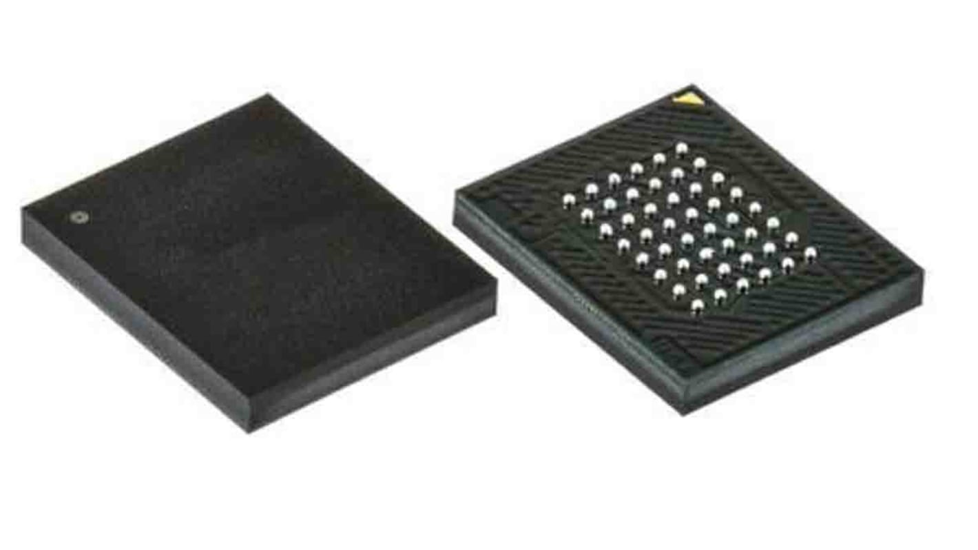
此圖片僅供參考,請參閲產品詳細資訊及規格
可享批量折扣
查看批量定價選項小計(1 托盤,共 338 件)*
TWD44,616.00
(不含稅)
TWD46,846.80
(含稅)
訂單超過 $1,300.00 免費送貨
暫時缺貨
- 從 2026年9月28日 發貨
**需要更多嗎?**輸入您需要的數量,然後按一下「查看送貨日期」以查詢更多庫存和送貨詳細資訊。
單位 | 每單位 | 每托盤* |
|---|---|---|
| 338 - 1352 | TWD132.00 | TWD44,616.00 |
| 1690 + | TWD128.00 | TWD43,264.00 |
* 參考價格
- RS庫存編號:
- 193-8825
- 製造零件編號:
- S29GL064S70BHI030
- 製造商:
- Infineon
規格
產品概覽和技術數據資料表
法例與合規
產品詳細資訊
透過選取一個或多個屬性來查找類似產品。
選取全部 | 屬性 | 值 |
|---|---|---|
| 品牌 | Infineon | |
| Memory Size | 64MB | |
| Product Type | Flash Memory | |
| Interface Type | CFI | |
| Package Type | BGA | |
| Pin Count | 48 | |
| Organisation | 8M x 8 bit | |
| Mount Type | Surface | |
| Cell Type | NOR | |
| Minimum Supply Voltage | 2.7V | |
| Maximum Supply Voltage | 3.6V | |
| Timing Type | Asynchronous | |
| Minimum Operating Temperature | -40°C | |
| Maximum Operating Temperature | 85°C | |
| Width | 6.15mm | |
| Height | 0.84mm | |
| Length | 8.15mm | |
| Standards/Approvals | No | |
| Series | S29GL064S | |
| Number of Words | 8K | |
| Automotive Standard | AEC-Q100 | |
| Supply Current | 50mA | |
| Number of Bits per Word | 8 | |
| Maximum Random Access Time | 70ns | |
| 選取全部 | ||
|---|---|---|
品牌 Infineon | ||
Memory Size 64MB | ||
Product Type Flash Memory | ||
Interface Type CFI | ||
Package Type BGA | ||
Pin Count 48 | ||
Organisation 8M x 8 bit | ||
Mount Type Surface | ||
Cell Type NOR | ||
Minimum Supply Voltage 2.7V | ||
Maximum Supply Voltage 3.6V | ||
Timing Type Asynchronous | ||
Minimum Operating Temperature -40°C | ||
Maximum Operating Temperature 85°C | ||
Width 6.15mm | ||
Height 0.84mm | ||
Length 8.15mm | ||
Standards/Approvals No | ||
Series S29GL064S | ||
Number of Words 8K | ||
Automotive Standard AEC-Q100 | ||
Supply Current 50mA | ||
Number of Bits per Word 8 | ||
Maximum Random Access Time 70ns | ||
The S29GL-S mid density family of devices are 3.0-volt single-power flash memory manufactured using 65 nm MirrorBit technology.
The S29GL064S is a 64-Mb device organized as 4,194,304 words or 8,388,608 bytes. Depending on the model number, the devices have 16bit wide data bus only, or a 16bit wide data bus that can also function as an 8bit wide data bus by using the BYTE# input.
The devices can be programmed either in the host system or in standard EPROM programmers. Access times as fast as 70 ns are available. Package offerings include 48pin TSOP, 56pin TSOP, 48-ball fine-pitch BGA, and 64-ball Fortified BGA, depending on model number. Each device has separate chip enable (CE#), write enable (WE#) and output enable (OE#) controls. Each device requires only a single 3.0-volt power supply for both read and write functions. In addition to a VCC input, a high-voltage accelerated program (ACC) feature is supported through increased voltage on the WP#/ACC or ACC input. This feature is intended to facilitate system production. Commands are written to the device using standard microprocessor write timing. Write cycles also internally latch addresses and data needed for the programming and erase operations.
The sector erase architecture allows memory sectors to be erased and reprogrammed without affecting the data contents of other sectors. The device is fully erased when shipped from the factory.
The Advanced Sector Protection features several levels of sector protection, which can disable both the program and erase operations in certain sectors.
相關連結
- Infineon NOR 64 MB CFI Flash Memory 48-Pin BGA, S29GL064S70BHI030
- Infineon NOR 256 MB CFI Flash Memory 64-Pin BGA
- Infineon NOR 256 MB CFI Flash Memory 64-Pin BGA, S29GL256P11FFIV20
- Infineon NOR 512 MB CFI, SPI Flash Memory 24-Pin BGA
- Infineon NOR 512 MB CFI S25FL512SAGBHID10
- Infineon NOR 512 MB CFI S25FL512SAGBHI310
- Infineon 512 MB CFI Flash Memory 64-Pin BGA, S29GL512T11FHIV20
- Infineon NOR 32 MB CFI Flash Memory 48-Pin TSOP