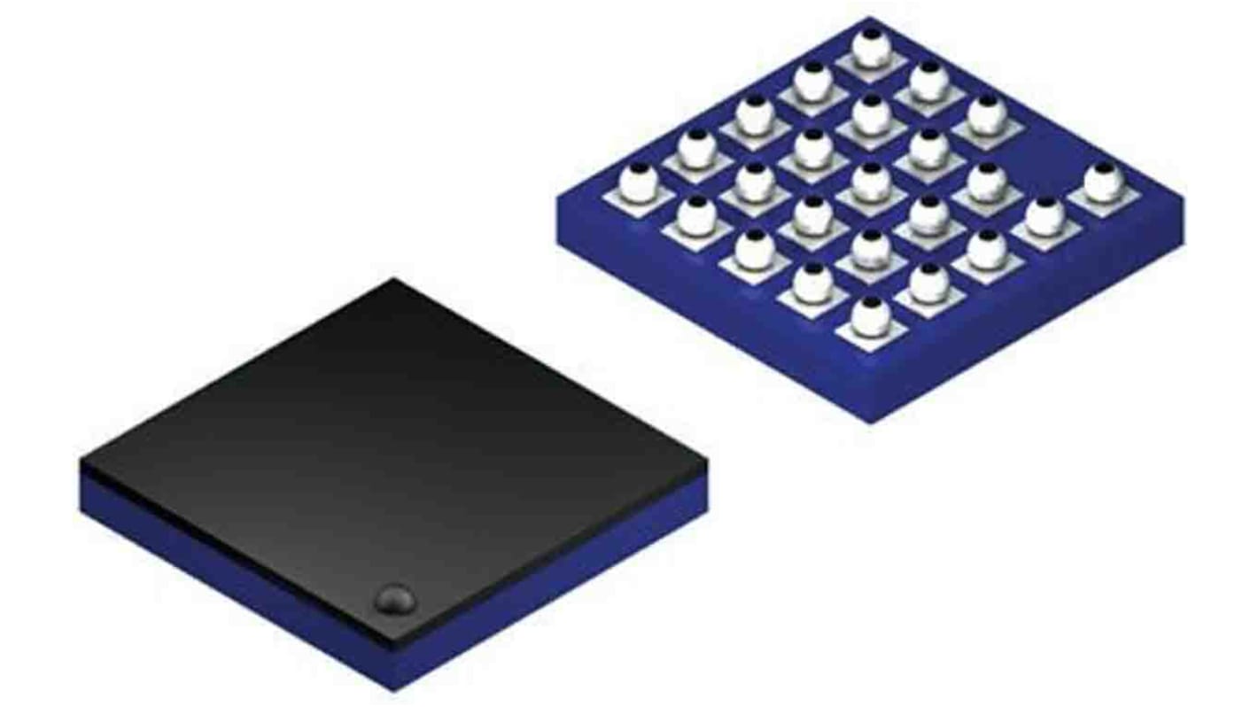
Infineon NOR 512 MB CFI, SPI Flash Memory 24-Pin BGA
- RS庫存編號:
- 193-8759
- 製造零件編號:
- S25FL512SAGBHI310
- 製造商:
- Infineon

此圖片僅供參考,請參閲產品詳細資訊及規格
可享批量折扣
小計(1 托盤,共 338 件)*
TWD65,166.40
(不含稅)
TWD68,424.72
(含稅)
訂單超過 $1,300.00 免費送貨
暫時缺貨
- 從 2026年7月27日 發貨
**需要更多嗎?**輸入您需要的數量,然後按一下「查看送貨日期」以查詢更多庫存和送貨詳細資訊。
單位 | 每單位 | 每托盤* |
|---|---|---|
| 338 - 1352 | TWD192.80 | TWD65,166.40 |
| 1690 + | TWD187.00 | TWD63,206.00 |
* 參考價格
- RS庫存編號:
- 193-8759
- 製造零件編號:
- S25FL512SAGBHI310
- 製造商:
- Infineon
規格
產品概覽和技術數據資料表
法例與合規
產品詳細資訊
透過選取一個或多個屬性來查找類似產品。
選取全部 | 屬性 | 值 |
|---|---|---|
| 品牌 | Infineon | |
| Memory Size | 512MB | |
| Product Type | Flash Memory | |
| Interface Type | CFI, SPI | |
| Package Type | BGA | |
| Pin Count | 24 | |
| Mount Type | Surface | |
| Maximum Clock Frequency | 133MHz | |
| Cell Type | NOR | |
| Minimum Supply Voltage | 1.65V | |
| Maximum Supply Voltage | 3.6V | |
| Minimum Operating Temperature | -40°C | |
| Maximum Operating Temperature | 85°C | |
| Height | 0.95mm | |
| Standards/Approvals | No | |
| Length | 8mm | |
| Automotive Standard | AEC-Q100 | |
| Number of Banks | 4 | |
| Number of Words | 64M | |
| Maximum Random Access Time | 14.5ns | |
| Number of Bits per Word | 8 | |
| Series | S25FL512S | |
| 選取全部 | ||
|---|---|---|
品牌 Infineon | ||
Memory Size 512MB | ||
Product Type Flash Memory | ||
Interface Type CFI, SPI | ||
Package Type BGA | ||
Pin Count 24 | ||
Mount Type Surface | ||
Maximum Clock Frequency 133MHz | ||
Cell Type NOR | ||
Minimum Supply Voltage 1.65V | ||
Maximum Supply Voltage 3.6V | ||
Minimum Operating Temperature -40°C | ||
Maximum Operating Temperature 85°C | ||
Height 0.95mm | ||
Standards/Approvals No | ||
Length 8mm | ||
Automotive Standard AEC-Q100 | ||
Number of Banks 4 | ||
Number of Words 64M | ||
Maximum Random Access Time 14.5ns | ||
Number of Bits per Word 8 | ||
Series S25FL512S | ||
This device connects to a host system via a Serial Peripheral Interface (SPI). Traditional SPI single bit serial input and output (SingleI/O or SIO) is supported as well as optional two bit (Dual I/O or DIO) and four bit (Quad I/O or QIO) serial commands. This multiplewidth interface is called SPI Multi-I/O or MIO. In addition, the FL-S family adds support for Double Data Rate (DDR) read commands for SIO, DIO and QIO that transfer address and read data on both edges of the clock.The Eclipse architecture features a Page Programming Buffer that allows up to 256 words (512 bytes) to be programmed in one operation, resulting in faster effective programming and erase than prior generation SPI program or erase algorithms. Executing code directly from flash memory is often called Execute-In-Place or XIP. By using FL-S devices at the higher clock rates supported, with QIO or DDR-QIO commands, the instruction read transfer rate can match or exceed traditional parallel interface,asynchronous, NOR flash memories while reducing signal count dramatically.The S25FL512S product offers high densities coupled with the flexibility and fast performance required by a variety of embedded applications. It is ideal for code shadowing, XIP and data storage.
相關連結
- Infineon NOR 512 MB CFI S25FL512SAGBHI310
- Infineon NOR 512 MB CFI, SPI Flash Memory 24-Pin BGA
- Infineon NOR 512 MB CFI S25FL512SAGBHID10
- Infineon NOR 512 MB SPI Flash Memory 24-Pin BGA
- Infineon NOR 512 MB SPI Flash Memory 24-Pin BGA, S25HL512TFABHI010
- Infineon NOR 512 MB SPI Flash Memory 24-Pin BGA, S26HL512TFPBHI010
- Infineon NOR 512 MB SPI Flash Memory 24-Pin BGA, S26HS512TGABHI010
- Infineon NOR 512 MB SPI Flash Memory 24-Pin BGA, S25HS512TFABHI010
