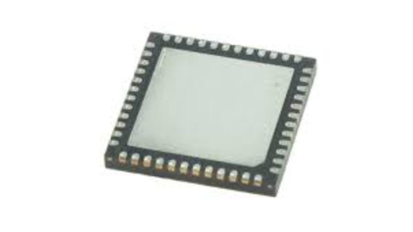
Renesas Electronics 9DBL0951BKILF Clock Buffer 48-Pin VFQFPN
- RS庫存編號:
- 250-3487
- 製造零件編號:
- 9DBL0951BKILF
- 製造商:
- Renesas Electronics

可享批量折扣
查看批量定價選項小計(1 包,共 2 件)*
TWD205.00
(不含稅)
TWD215.24
(含稅)
訂單超過 $1,300.00 免費送貨
有庫存
- 306 件準備從其他地點送貨
**需要更多嗎?**輸入您需要的數量,然後按一下「查看送貨日期」以查詢更多庫存和送貨詳細資訊。
單位 | 每單位 | 每包* |
|---|---|---|
| 2 - 8 | TWD102.50 | TWD205.00 |
| 10 - 18 | TWD100.50 | TWD201.00 |
| 20 - 98 | TWD98.00 | TWD196.00 |
| 100 - 198 | TWD96.50 | TWD193.00 |
| 200 + | TWD94.00 | TWD188.00 |
* 參考價格
- RS庫存編號:
- 250-3487
- 製造零件編號:
- 9DBL0951BKILF
- 製造商:
- Renesas Electronics
規格
產品概覽和技術數據資料表
法例與合規
產品詳細資訊
透過選取一個或多個屬性來查找類似產品。
選取全部 | 屬性 | 值 |
|---|---|---|
| 品牌 | Renesas Electronics | |
| Product Type | Clock Buffer | |
| Maximum Input Frequency | 200MHz | |
| Mount Type | Surface | |
| Package Type | VFQFPN | |
| Pin Count | 48 | |
| Minimum Supply Voltage | 3.14V | |
| Maximum Supply Voltage | 3.47V | |
| Minimum Operating Temperature | -40°C | |
| Maximum Operating Temperature | 85°C | |
| Height | 1mm | |
| Series | 9DBL09x1 | |
| Standards/Approvals | RoHS | |
| Length | 6mm | |
| Automotive Standard | No | |
| 選取全部 | ||
|---|---|---|
品牌 Renesas Electronics | ||
Product Type Clock Buffer | ||
Maximum Input Frequency 200MHz | ||
Mount Type Surface | ||
Package Type VFQFPN | ||
Pin Count 48 | ||
Minimum Supply Voltage 3.14V | ||
Maximum Supply Voltage 3.47V | ||
Minimum Operating Temperature -40°C | ||
Maximum Operating Temperature 85°C | ||
Height 1mm | ||
Series 9DBL09x1 | ||
Standards/Approvals RoHS | ||
Length 6mm | ||
Automotive Standard No | ||
The Renesas Electronics fan-out buffers are 3.3V members of IDT's full featured PCIe clock family. This devices support PCIe Gen1–4 Common Clocked (CC) and PCIe
Separate Reference Independent Spread (SRIS) systems. They offer a choice of integrated output terminations providing direct connection to 85Ω or 100Ω transmission lines. It can be factory programmed with a user-defined power up default SMBus configuration. Various applications where this device is used are PCIe Gen1–4 clock distribution for Riser Cards, Storage, Networking, JBOD, Communications and Access Points.
Direct connection to 100ohm or 85ohm transmission lines saves 36 resistors compared to standard PCIe devices
165mW of typical power consumption at 3.3V eliminates thermal concerns
VDDIO allows 50% power savings at optional 1.05V
Customer defined SMBus power up default can be programmed into P1 device
HCSL differential input can be driven by common clock sources
Spread spectrum tolerant allows reduction of EMI
Device contains default configuration
Three selectable SMBus addresses so multiple devices can easily share an SMBus segment
Space saving 48-pin 6 x 6mm VFQFPN
相關連結
- Renesas Electronics 9DBL0951BKILF Clock Buffer 48-Pin VFQFPN
- Renesas Electronics 9DBV0831AKILF Clock Buffer 48-Pin VFQFPN
- Renesas Electronics 9ZXL0831EKILF Clock Buffer 48-Pin VFQFPN
- Renesas Electronics 9DBV0841AKLF Clock Buffer 48-Pin VFQFPN
- Renesas Electronics 9ZXL0852EKILF Clock Buffer 48-Pin VFQFPN
- Renesas Electronics 8P34S1208NBGI Clock Buffer 28-Pin VFQFPN
- Renesas Electronics 5P1103A000NLGI Clock Buffer 24-Pin VFQFPN
- Renesas Electronics 9DML4493ANLGI Clock Buffer 32-Pin VFQFPN