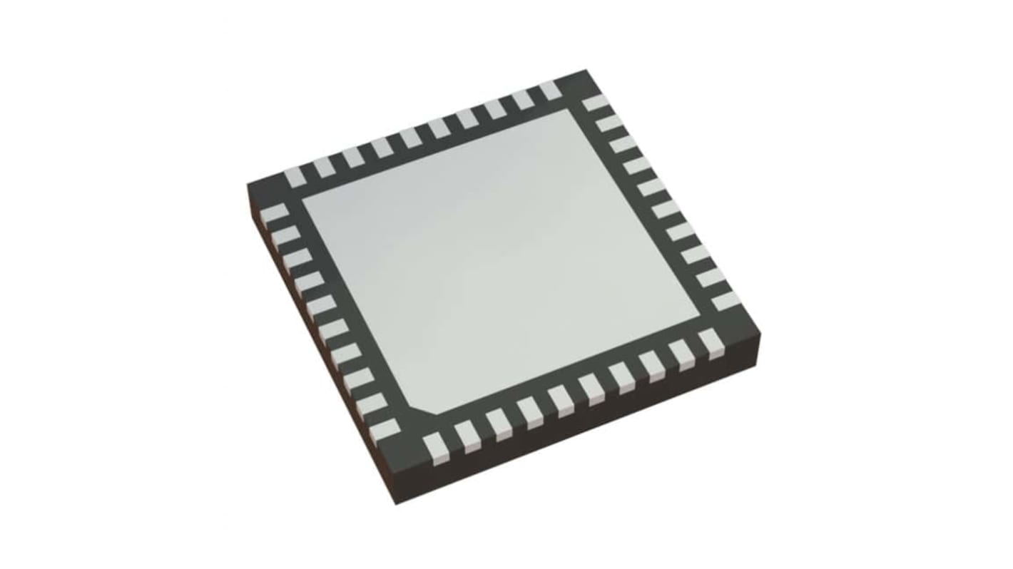
Renesas Electronics 8T49N242-999NLGI Clock Buffer 40-Pin VFQFN
- RS庫存編號:
- 250-3483
- 製造零件編號:
- 8T49N242-999NLGI
- 製造商:
- Renesas Electronics

此圖片僅供參考,請參閲產品詳細資訊及規格
暫時無法供應
我們無法確定此產品何時有貨,RS 預計將其從我們的產品目錄中移除。
- RS庫存編號:
- 250-3483
- 製造零件編號:
- 8T49N242-999NLGI
- 製造商:
- Renesas Electronics
規格
產品概覽和技術數據資料表
法例與合規
產品詳細資訊
透過選取一個或多個屬性來查找類似產品。
選取全部 | 屬性 | 值 |
|---|---|---|
| 品牌 | Renesas Electronics | |
| Product Type | Clock Buffer | |
| Maximum Input Frequency | 875MHz | |
| Mount Type | Surface | |
| Package Type | VFQFN | |
| Pin Count | 40 | |
| Number of Outputs | 9 | |
| Minimum Supply Voltage | 3.14V | |
| Maximum Supply Voltage | 3.47V | |
| Minimum Operating Temperature | -40°C | |
| Maximum Operating Temperature | 85°C | |
| Series | 8T49N242 | |
| Length | 6mm | |
| Width | 6 mm | |
| Standards/Approvals | RoHS | |
| Height | 1mm | |
| Automotive Standard | No | |
| 選取全部 | ||
|---|---|---|
品牌 Renesas Electronics | ||
Product Type Clock Buffer | ||
Maximum Input Frequency 875MHz | ||
Mount Type Surface | ||
Package Type VFQFN | ||
Pin Count 40 | ||
Number of Outputs 9 | ||
Minimum Supply Voltage 3.14V | ||
Maximum Supply Voltage 3.47V | ||
Minimum Operating Temperature -40°C | ||
Maximum Operating Temperature 85°C | ||
Series 8T49N242 | ||
Length 6mm | ||
Width 6 mm | ||
Standards/Approvals RoHS | ||
Height 1mm | ||
Automotive Standard No | ||
The Renesas Electronics frequency translator has one fractional-feedback PLL that can be used as a jitter attenuator and frequency translator. It is equipped with four integer output dividers, allowing the generation of up to four different output frequencies, ranging from 8kHz to 1GHz. These frequencies are completely independent of the input reference frequencies, and the crystal reference frequency. The outputs may select among LVPECL, LVDS, HCSL or LVCMOS output levels.
It accepts up to two differential or single-ended input clocks and a fundamental-mode crystal input
The internal PLL can lock to either of the input reference clocks or just to the crystal to behave as a frequency synthesizer
The device supports hitless reference switching between input clocks
The device monitors both input clocks for Loss of Signal and generates an alarm when an input clock failure is detected
The PLL has a register-selectable loop bandwidth from 0.2Hz to 6.4kHz
The device is programmable through an I2C interface
It also supports I2C master capability to allow the register configuration to be read from an external EEPROM
