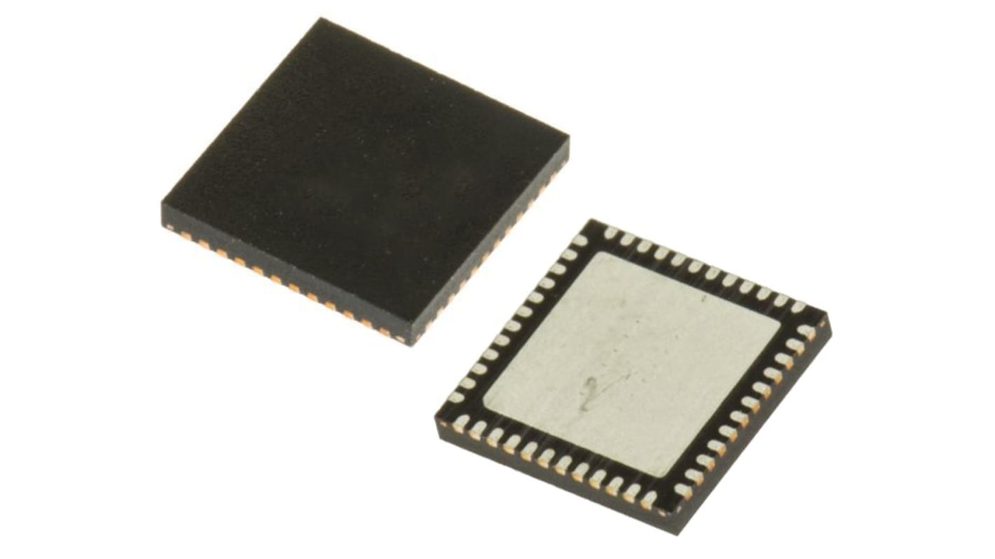
Renesas Electronics 8T39S11ANLGI Clock Buffer 48-Pin VFQFN-48
- RS庫存編號:
- 264-3519
- 製造零件編號:
- 8T39S11ANLGI
- 製造商:
- Renesas Electronics

暫時無法供應
我們不知道此物品是否會到貨,因為製造商正在對其逐步停產。
- RS庫存編號:
- 264-3519
- 製造零件編號:
- 8T39S11ANLGI
- 製造商:
- Renesas Electronics
規格
產品概覽和技術數據資料表
法例與合規
產品詳細資訊
透過選取一個或多個屬性來查找類似產品。
選取全部 | 屬性 | 值 |
|---|---|---|
| 品牌 | Renesas Electronics | |
| Product Type | Clock Buffer | |
| Maximum Input Frequency | 40MHz | |
| Mount Type | Surface | |
| Maximum Propagation Delay Time | 2.65ns | |
| Package Type | VFQFN-48 | |
| Pin Count | 48 | |
| Minimum Supply Voltage | 2.5V | |
| Maximum Supply Voltage | 3.3V | |
| Minimum Operating Temperature | -40°C | |
| Maximum Operating Temperature | 85°C | |
| Standards/Approvals | RoHS | |
| Height | 0.85mm | |
| Length | 7mm | |
| Series | 8T39S11A | |
| Automotive Standard | No | |
| 選取全部 | ||
|---|---|---|
品牌 Renesas Electronics | ||
Product Type Clock Buffer | ||
Maximum Input Frequency 40MHz | ||
Mount Type Surface | ||
Maximum Propagation Delay Time 2.65ns | ||
Package Type VFQFN-48 | ||
Pin Count 48 | ||
Minimum Supply Voltage 2.5V | ||
Maximum Supply Voltage 3.3V | ||
Minimum Operating Temperature -40°C | ||
Maximum Operating Temperature 85°C | ||
Standards/Approvals RoHS | ||
Height 0.85mm | ||
Length 7mm | ||
Series 8T39S11A | ||
Automotive Standard No | ||
- COO (Country of Origin):
- TH
The Renesas Electronics Crystal or differential to Differential is a high performance clock fan-out buffer. The input clock can be selected from two differential inputs or one crystal input. The internal oscillator circuit is automatically disabled if the crystal input is not selected. The crystal pin can be driven by a single ended clock. The selected signal is distributed to ten differential outputs which can be configured as LVPECL LVDS or HSCL outputs. All outputs can be disabled into a high impedance state.
48 Lead VFQFN with lead free package available
Two differential reference clock input pairs
Crystal Input accepts 10MHz to 40MHz Crystal or Single Ended clock
Two banks and each has five differential output pairs that can be configured as LVPECL or LVDS or HCSL
相關連結
- Renesas Electronics 8T39S11ANLGI Clock Buffer 48-Pin VFQFN-48
- Renesas Electronics 9FGV0231AKLF Clock Buffer 24-Pin VFQFN
- Renesas Electronics 5PB1102CMGK Clock Buffer 8-Pin VFQFN
- Renesas Electronics 9DB803DFLFT Clock Buffer 48-Pin SSOP-48
- Renesas Electronics Clock Buffer 48-Pin TSSOP
- Renesas Electronics 9DBV0831AKILF Clock Buffer 48-Pin VFQFPN
- Renesas Electronics 9DB803DFILF Clock Buffer 48-Pin SSOP
- Renesas Electronics 9DBL0951BKILF Clock Buffer 48-Pin VFQFPN