onsemi Type N-Channel MOSFET, 40 A, 650 V Enhancement, 3-Pin TO-220
- RS庫存編號:
- 178-4258
- 製造零件編號:
- NTPF082N65S3F
- 製造商:
- onsemi

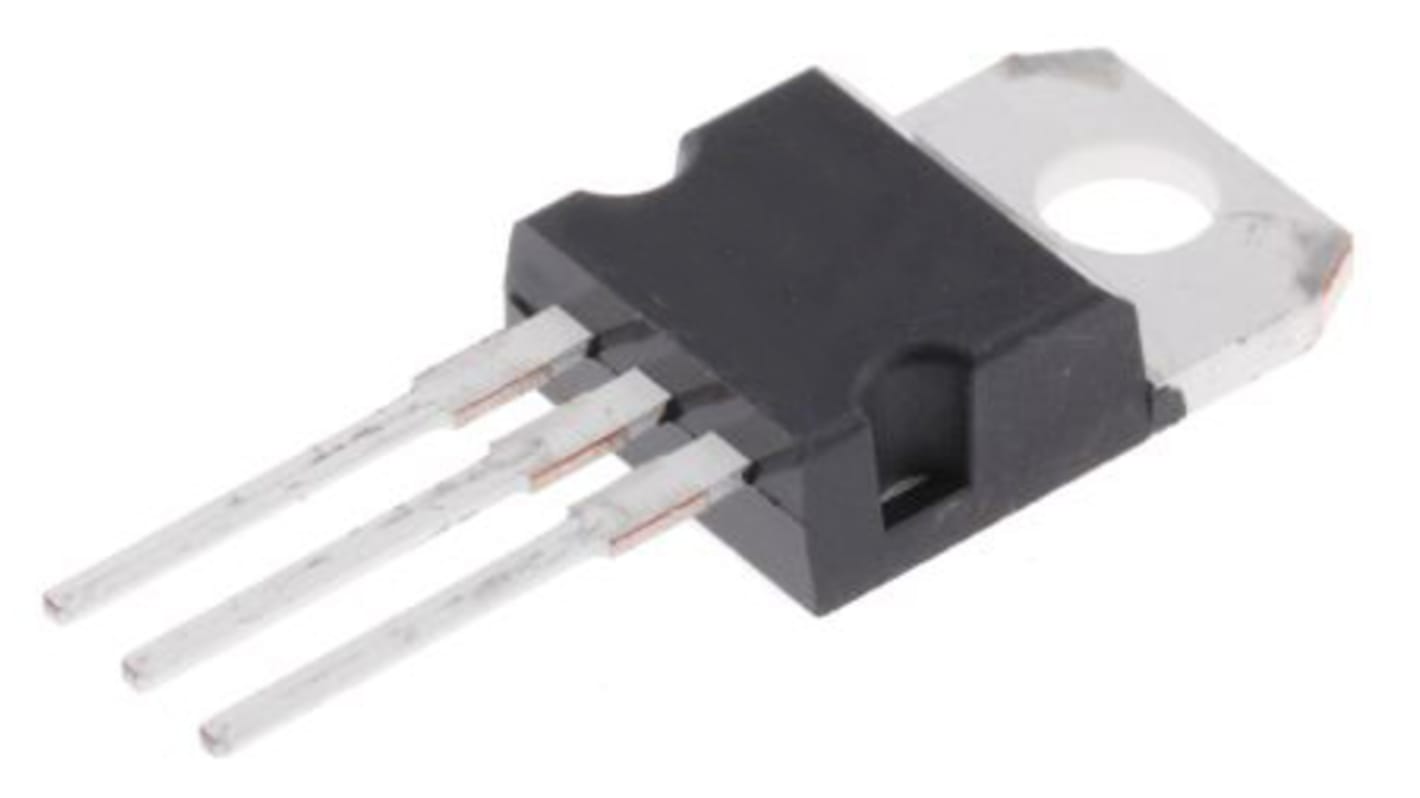
此圖片僅供參考,請參閲產品詳細資訊及規格
可享批量折扣
查看批量定價選項小計(1 管,共 50 件)*
TWD7,270.00
(不含稅)
TWD7,633.50
(含稅)
訂單超過 $1,300.00 免費送貨
最後的 RS 庫存
- 最終 250 個,準備發貨
單位 | 每單位 | 每管* |
|---|---|---|
| 50 - 50 | TWD145.40 | TWD7,270.00 |
| 100 - 150 | TWD142.40 | TWD7,120.00 |
| 200 + | TWD139.60 | TWD6,980.00 |
* 參考價格
- RS庫存編號:
- 178-4258
- 製造零件編號:
- NTPF082N65S3F
- 製造商:
- onsemi
規格
產品概覽和技術數據資料表
法例與合規
產品詳細資訊
透過選取一個或多個屬性來查找類似產品。
選取全部 | 屬性 | 值 |
|---|---|---|
| 品牌 | onsemi | |
| Product Type | MOSFET | |
| Channel Type | Type N | |
| Maximum Continuous Drain Current Id | 40A | |
| Maximum Drain Source Voltage Vds | 650V | |
| Package Type | TO-220 | |
| Mount Type | Through Hole | |
| Pin Count | 3 | |
| Maximum Drain Source Resistance Rds | 82mΩ | |
| Channel Mode | Enhancement | |
| Minimum Operating Temperature | -55°C | |
| Forward Voltage Vf | 1.3V | |
| Maximum Power Dissipation Pd | 48W | |
| Typical Gate Charge Qg @ Vgs | 70nC | |
| Maximum Operating Temperature | 150°C | |
| Standards/Approvals | No | |
| Height | 16.12mm | |
| Length | 10.63mm | |
| Automotive Standard | No | |
| 選取全部 | ||
|---|---|---|
品牌 onsemi | ||
Product Type MOSFET | ||
Channel Type Type N | ||
Maximum Continuous Drain Current Id 40A | ||
Maximum Drain Source Voltage Vds 650V | ||
Package Type TO-220 | ||
Mount Type Through Hole | ||
Pin Count 3 | ||
Maximum Drain Source Resistance Rds 82mΩ | ||
Channel Mode Enhancement | ||
Minimum Operating Temperature -55°C | ||
Forward Voltage Vf 1.3V | ||
Maximum Power Dissipation Pd 48W | ||
Typical Gate Charge Qg @ Vgs 70nC | ||
Maximum Operating Temperature 150°C | ||
Standards/Approvals No | ||
Height 16.12mm | ||
Length 10.63mm | ||
Automotive Standard No | ||
- COO (Country of Origin):
- CN
SUPERFET III MOSFET is ON Semiconductor’s brand−new high voltage super−junction (SJ) MOSFET family that is utilizing charge balance technology for outstanding low on−resistance and lower gate charge performance. This advanced technology is tailored to minimize conduction loss, provide superior switching performance, and withstand extreme dv/dt rate.
Features
700 V @ TJ = 150 oC
Ultra Low Gate Charge (Typ. Qg = 70 nC)
Low Effective Output Capacitance (Typ. Coss(eff.) = 680 pF)
Optimized Capacitance
Excellent body diode performance (low Qrr, robust body diode)
Typ. RDS(on) = 70 mΩ
Higher system reliability at low temperature operation
Lower switching loss
Lower switching loss
Lower peak Vds and lower Vgs oscillation
Higher system reliability in LLC and Phase shift full bridge Circuit
Applications
Telecommunication
Cloud system
Industrial
End Products
Telecom power
Server power
Solar / UPS
EV charger
相關連結
- onsemi Type N-Channel MOSFET 650 V Enhancement, 3-Pin TO-220 NTPF082N65S3F
- onsemi NTP Type N-Channel MOSFET 650 V Enhancement, 3-Pin TO-220
- onsemi NTP067N Type N-Channel MOSFET 650 V Enhancement, 3-Pin TO-220
- onsemi Type N-Channel MOSFET 650 V Enhancement, 3-Pin TO-220
- onsemi Type N-Channel MOSFET 650 V Enhancement, 3-Pin TO-220
- onsemi Type N-Channel MOSFET 650 V Enhancement, 3-Pin TO-220
- onsemi NTP067N Type N-Channel MOSFET 650 V Enhancement, 3-Pin TO-220 NTP067N65S3H
- onsemi NTP Type N-Channel MOSFET 650 V Enhancement, 3-Pin TO-220 NTP082N65S3HF