onsemi QFET Type P-Channel MOSFET, 11.5 A, 200 V Enhancement, 3-Pin TO-263
- RS庫存編號:
- 166-2528
- 製造零件編號:
- FQB12P20TM
- 製造商:
- onsemi

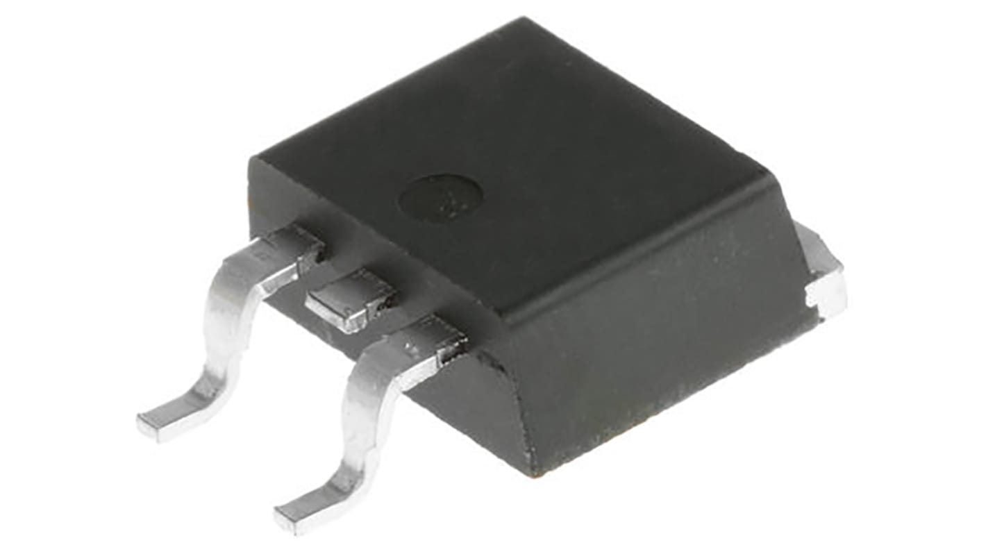
此圖片僅供參考,請參閲產品詳細資訊及規格
可享批量折扣
查看批量定價選項小計(1 卷,共 800 件)*
TWD26,640.00
(不含稅)
TWD27,968.00
(含稅)
訂單超過 $1,300.00 免費送貨
暫時缺貨
- 從 2026年10月05日 發貨
**需要更多嗎?**輸入您需要的數量,然後按一下「查看送貨日期」以查詢更多庫存和送貨詳細資訊。
單位 | 每單位 | 每卷* |
|---|---|---|
| 800 - 3200 | TWD33.30 | TWD26,640.00 |
| 4000 + | TWD31.60 | TWD25,280.00 |
* 參考價格
- RS庫存編號:
- 166-2528
- 製造零件編號:
- FQB12P20TM
- 製造商:
- onsemi
規格
產品概覽和技術數據資料表
法例與合規
產品詳細資訊
透過選取一個或多個屬性來查找類似產品。
選取全部 | 屬性 | 值 |
|---|---|---|
| 品牌 | onsemi | |
| Product Type | MOSFET | |
| Channel Type | Type P | |
| Maximum Continuous Drain Current Id | 11.5A | |
| Maximum Drain Source Voltage Vds | 200V | |
| Series | QFET | |
| Package Type | TO-263 | |
| Mount Type | Surface | |
| Pin Count | 3 | |
| Maximum Drain Source Resistance Rds | 470mΩ | |
| Channel Mode | Enhancement | |
| Typical Gate Charge Qg @ Vgs | 31nC | |
| Maximum Power Dissipation Pd | 3.13W | |
| Minimum Operating Temperature | -55°C | |
| Forward Voltage Vf | -5V | |
| Maximum Operating Temperature | 150°C | |
| Height | 4.83mm | |
| Standards/Approvals | No | |
| Length | 10.67mm | |
| Automotive Standard | No | |
| 選取全部 | ||
|---|---|---|
品牌 onsemi | ||
Product Type MOSFET | ||
Channel Type Type P | ||
Maximum Continuous Drain Current Id 11.5A | ||
Maximum Drain Source Voltage Vds 200V | ||
Series QFET | ||
Package Type TO-263 | ||
Mount Type Surface | ||
Pin Count 3 | ||
Maximum Drain Source Resistance Rds 470mΩ | ||
Channel Mode Enhancement | ||
Typical Gate Charge Qg @ Vgs 31nC | ||
Maximum Power Dissipation Pd 3.13W | ||
Minimum Operating Temperature -55°C | ||
Forward Voltage Vf -5V | ||
Maximum Operating Temperature 150°C | ||
Height 4.83mm | ||
Standards/Approvals No | ||
Length 10.67mm | ||
Automotive Standard No | ||
Enhancement Mode P-Channel MOSFET, ON Semiconductor
ON Semiconductors range of P-Channel MOSFETS are produced using ON Semi’s proprietary, high cell density, DMOS technology. This very high density process has been designed to minimize on-state resistance to provide a rugged and reliable performance for fast switching.
Features and Benefits:
• Voltage controlled P-Channel small signal switch
• High-Density cell design
• High saturation current
• Superior switching
• Great rugged and reliable performance
• DMOS technology
Applications:
• Load Switching
• DC/DC converter
• Battery protection
• Power management control
• DC motor control
MOSFET Transistors, ON Semi
ON Semi offers a substantial portfolio of MOSFET devices that includes high-voltage (>250V) and low-voltage (<250V) types. The Advanced silicon technology provides smaller die sizes, which it is incorporated into multiple industry-standard and thermally-enhanced packages.
ON Semi MOSFETs provide superior design reliability from reduced voltage spikes and overshoot, to lower junction capacitance and reverse recovery charge, to elimination of additional external components to keep systems up and running longer.
相關連結
- onsemi QFET Type P-Channel MOSFET 200 V Enhancement, 3-Pin TO-263 FQB12P20TM
- onsemi QFET Type P-Channel MOSFET 100 V Enhancement, 3-Pin TO-263
- onsemi QFET Type P-Channel MOSFET 100 V Enhancement, 3-Pin TO-263
- onsemi QFET Type P-Channel MOSFET 60 V Enhancement, 3-Pin TO-263
- onsemi QFET Type P-Channel MOSFET 60 V Enhancement, 3-Pin TO-263 FQB27P06TM
- onsemi QFET Type P-Channel MOSFET 100 V Enhancement, 3-Pin TO-263 FQB22P10TM
- onsemi QFET Type P-Channel MOSFET 100 V Enhancement, 3-Pin TO-263 FQB34P10TM
- onsemi QFET Type P-Channel MOSFET 60 V Enhancement, 3-Pin TO-263 FQB47P06TM-AM002