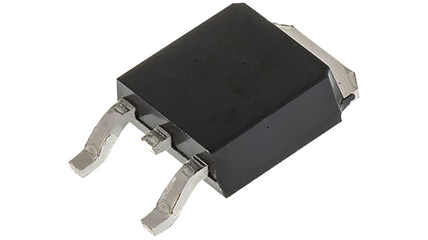
onsemi PowerTrench Type P-Channel MOSFET, 6.7 A, 12 V Enhancement, 3-Pin TO-252
- RS庫存編號:
- 166-2398
- 製造零件編號:
- FDD306P
- 製造商:
- onsemi

此圖片僅供參考,請參閲產品詳細資訊及規格
可享批量折扣
小計(1 卷,共 2500 件)*
TWD33,750.00
(不含稅)
TWD35,450.00
(含稅)
訂單超過 $1,300.00 免費送貨
暫時缺貨
- 從 2026年6月26日 發貨
**需要更多嗎?**輸入您需要的數量,然後按一下「查看送貨日期」以查詢更多庫存和送貨詳細資訊。
單位 | 每單位 | 每卷* |
|---|---|---|
| 2500 - 2500 | TWD13.50 | TWD33,750.00 |
| 5000 + | TWD13.10 | TWD32,750.00 |
* 參考價格
- RS庫存編號:
- 166-2398
- 製造零件編號:
- FDD306P
- 製造商:
- onsemi
規格
產品概覽和技術數據資料表
法例與合規
產品詳細資訊
透過選取一個或多個屬性來查找類似產品。
選取全部 | 屬性 | 值 |
|---|---|---|
| 品牌 | onsemi | |
| Channel Type | Type P | |
| Product Type | MOSFET | |
| Maximum Continuous Drain Current Id | 6.7A | |
| Maximum Drain Source Voltage Vds | 12V | |
| Series | PowerTrench | |
| Package Type | TO-252 | |
| Mount Type | Surface | |
| Pin Count | 3 | |
| Maximum Drain Source Resistance Rds | 90mΩ | |
| Channel Mode | Enhancement | |
| Forward Voltage Vf | -1.2V | |
| Maximum Power Dissipation Pd | 52W | |
| Minimum Operating Temperature | -55°C | |
| Typical Gate Charge Qg @ Vgs | 15nC | |
| Maximum Gate Source Voltage Vgs | 8 V | |
| Maximum Operating Temperature | 175°C | |
| Height | 2.39mm | |
| Width | 6.22 mm | |
| Standards/Approvals | No | |
| Length | 6.73mm | |
| Automotive Standard | No | |
| 選取全部 | ||
|---|---|---|
品牌 onsemi | ||
Channel Type Type P | ||
Product Type MOSFET | ||
Maximum Continuous Drain Current Id 6.7A | ||
Maximum Drain Source Voltage Vds 12V | ||
Series PowerTrench | ||
Package Type TO-252 | ||
Mount Type Surface | ||
Pin Count 3 | ||
Maximum Drain Source Resistance Rds 90mΩ | ||
Channel Mode Enhancement | ||
Forward Voltage Vf -1.2V | ||
Maximum Power Dissipation Pd 52W | ||
Minimum Operating Temperature -55°C | ||
Typical Gate Charge Qg @ Vgs 15nC | ||
Maximum Gate Source Voltage Vgs 8 V | ||
Maximum Operating Temperature 175°C | ||
Height 2.39mm | ||
Width 6.22 mm | ||
Standards/Approvals No | ||
Length 6.73mm | ||
Automotive Standard No | ||
PowerTrench® P-Channel MOSFET, Fairchild Semiconductor
PowerTrench® MOSFETs are optimised power switches that offer increase of system efficiency and power density. They combine small gate charge(Qg), small reverse recovery charge(Qrr) and soft reverse recovery body diode, which contributes to fast switching of synchronous rectification in AC/DC power supplies.
The latest PowerTrench® MOSFETs employa shielded-gate structure that provides charge balance. By utilizing this Advanced technology, the FOM (Figure of Merit) of these devices is significant lower than that of previous generations.
Soft body diode performance of the PowerTrench® MOSFETs is able to eliminate snubber circuits or replace a higher voltage rating MOSFET.
MOSFET Transistors, ON Semi
ON Semi offers a substantial portfolio of MOSFET devices that includes high-voltage (>250V) and low-voltage (<250V) types. The Advanced silicon technology provides smaller die sizes, which it is incorporated into multiple industry-standard and thermally-enhanced packages.
ON Semi MOSFETs provide superior design reliability from reduced voltage spikes and overshoot, to lower junction capacitance and reverse recovery charge, to elimination of additional external components to keep systems up and running longer.
相關連結
- onsemi PowerTrench Type P-Channel MOSFET 12 V Enhancement, 3-Pin TO-252 FDD306P
- onsemi PowerTrench Type P-Channel MOSFET 40 V Enhancement, 3-Pin TO-252
- onsemi PowerTrench Type P-Channel MOSFET 40 V Enhancement, 3-Pin TO-252 FDD4243
- onsemi PowerTrench Type P-Channel PowerTrench MOSFET 40 V Enhancement, 3-Pin TO-252
- onsemi PowerTrench Type P-Channel PowerTrench MOSFET 40 V Enhancement, 3-Pin TO-252 FDD4141
- onsemi PowerTrench Type P-Channel MOSFET 30 V Enhancement, 3-Pin TO-252
- onsemi PowerTrench Type P-Channel MOSFET 35 V Enhancement, 3-Pin TO-252
- onsemi PowerTrench Type P-Channel MOSFET 40 V Enhancement, 3-Pin TO-252
