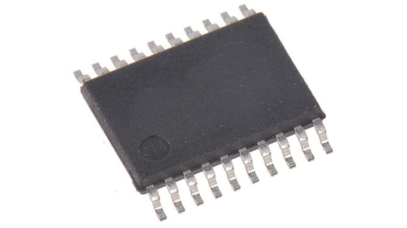
Renesas Electronics 9DB102BGILF, LVDS Buffer 2 TTL Buffer, 20-Pin TSSOP
- RS庫存編號:
- 217-7929
- 製造零件編號:
- 9DB102BGILF
- 製造商:
- Renesas Electronics

可享批量折扣
查看批量定價選項小計(1 包,共 5 件)*
TWD746.00
(不含稅)
TWD783.30
(含稅)
訂單超過 $1,300.00 免費送貨
有庫存
- 加上 45 件從 2026年7月27日 起發貨
**需要更多嗎?**輸入您需要的數量,然後按一下「查看送貨日期」以查詢更多庫存和送貨詳細資訊。
單位 | 每單位 | 每包* |
|---|---|---|
| 5 - 15 | TWD149.20 | TWD746.00 |
| 20 - 30 | TWD145.40 | TWD727.00 |
| 35 + | TWD143.20 | TWD716.00 |
* 參考價格
- RS庫存編號:
- 217-7929
- 製造零件編號:
- 9DB102BGILF
- 製造商:
- Renesas Electronics
規格
產品概覽和技術數據資料表
法例與合規
產品詳細資訊
透過選取一個或多個屬性來查找類似產品。
選取全部 | 屬性 | 值 |
|---|---|---|
| 品牌 | Renesas Electronics | |
| Product Type | LVDS Buffer | |
| Number of Drivers | 2 | |
| Input Type | TTL | |
| Output Type | Buffer | |
| Sub Type | Buffer | |
| Number of Elements per Chip | 2 | |
| Mount Type | Surface | |
| Package Type | TSSOP | |
| Pin Count | 20 | |
| Minimum Supply Voltage | 3V | |
| Maximum Supply Voltage | 3.3V | |
| ESD Protection | Yes | |
| Minimum Operating Temperature | -40°C | |
| Maximum Operating Temperature | 85°C | |
| Series | 9DB102 | |
| Height | 1.05mm | |
| Length | 6.6mm | |
| Standards/Approvals | No | |
| Automotive Standard | No | |
| 選取全部 | ||
|---|---|---|
品牌 Renesas Electronics | ||
Product Type LVDS Buffer | ||
Number of Drivers 2 | ||
Input Type TTL | ||
Output Type Buffer | ||
Sub Type Buffer | ||
Number of Elements per Chip 2 | ||
Mount Type Surface | ||
Package Type TSSOP | ||
Pin Count 20 | ||
Minimum Supply Voltage 3V | ||
Maximum Supply Voltage 3.3V | ||
ESD Protection Yes | ||
Minimum Operating Temperature -40°C | ||
Maximum Operating Temperature 85°C | ||
Series 9DB102 | ||
Height 1.05mm | ||
Length 6.6mm | ||
Standards/Approvals No | ||
Automotive Standard No | ||
The Renesas Electronics 9DB102 zero-delay buffer supports PCI Express clocking requirements. The 9DB102 is driven by a differential SRC output pair from an IDT CK409/CK410-compliant main clock generator such as the 952601 or 954101. It attenuates jitter on the input clock and has a selectable PLL Band Width to maximize performance in systems with or without Spread- Spectrum clocking.
2 - 0.7 V HCSL differential output pairs
Phase jitter: PCIe Gen2 < 3.1 ps rms
Phase jitter: PCIe Gen1 < 86 ps peak to peak
Supports zero delay buffer mode and fanout mode
Bandwidth programming available
33-110 MHz operation in PLL mode
10-110 MHz operation in Bypass mode
相關連結
- Renesas Electronics 9DB102BGILF 20-Pin TSSOP
- Renesas Electronics Line Transceiver 20-Pin TSSOP
- Renesas Electronics ICL3223EIVZ 20-Channel Line Transceiver 20-Pin TSSOP
- Renesas Electronics ICL3222EIVZ-T Line Transceiver 20-Pin TSSOP
- Renesas Electronics Clock Buffer 20-Pin TSSOP
- Texas Instruments LVTTL, 16-Pin TSSOP
- Texas Instruments CMOS LVDS, 48-Pin TSSOP
- Texas Instruments CMOS LVDS, 16-Pin TSSOP