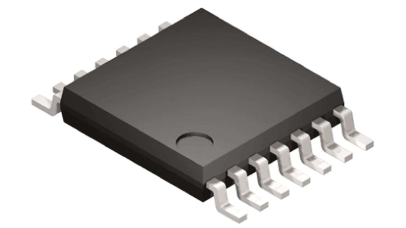
Nexperia 74LVC125APW,112, 4 4-Input Buffer & Line Driver Logic Gate, 14-Pin TSSOP
- RS庫存編號:
- 124-2270
- 製造零件編號:
- 74LVC125APW,112
- 製造商:
- Nexperia

此圖片僅供參考,請參閲產品詳細資訊及規格
可享批量折扣
小計(1 管,共 96 件)*
TWD489.60
(不含稅)
TWD514.56
(含稅)
訂單超過 $1,300.00 免費送貨
暫時缺貨
- 7,872 件從 2026年5月21日 起裝運發貨
**需要更多嗎?**輸入您需要的數量,然後按一下「查看送貨日期」以查詢更多庫存和送貨詳細資訊。
單位 | 每單位 | 每管* |
|---|---|---|
| 96 - 96 | TWD5.10 | TWD489.60 |
| 192 - 384 | TWD4.90 | TWD470.40 |
| 480 + | TWD4.80 | TWD460.80 |
* 參考價格
- RS庫存編號:
- 124-2270
- 製造零件編號:
- 74LVC125APW,112
- 製造商:
- Nexperia
規格
產品概覽和技術數據資料表
法例與合規
產品詳細資訊
透過選取一個或多個屬性來查找類似產品。
選取全部 | 屬性 | 值 |
|---|---|---|
| 品牌 | Nexperia | |
| Product Type | Logic Gate | |
| Logic Function | Buffer & Line Driver | |
| Mount Type | Surface | |
| Number of Elements | 4 | |
| Number of Inputs per Gate | 4 | |
| Schmitt Trigger Input | No | |
| Package Type | TSSOP | |
| Pin Count | 14 | |
| Logic Family | LVC | |
| Input Type | Single Ended | |
| Minimum Operating Temperature | -40°C | |
| Maximum Propagation Delay Time @ CL | 6ns | |
| Maximum High Level Output Current | -24mA | |
| Maximum Operating Temperature | 125°C | |
| Standards/Approvals | No | |
| Length | 5.1mm | |
| Maximum Supply Voltage | 3.6V | |
| Height | 0.95mm | |
| Minimum Supply Voltage | 1.2V | |
| Maximum Low Level Output Current | 24mA | |
| Automotive Standard | No | |
| Output Type | 3 State | |
| 選取全部 | ||
|---|---|---|
品牌 Nexperia | ||
Product Type Logic Gate | ||
Logic Function Buffer & Line Driver | ||
Mount Type Surface | ||
Number of Elements 4 | ||
Number of Inputs per Gate 4 | ||
Schmitt Trigger Input No | ||
Package Type TSSOP | ||
Pin Count 14 | ||
Logic Family LVC | ||
Input Type Single Ended | ||
Minimum Operating Temperature -40°C | ||
Maximum Propagation Delay Time @ CL 6ns | ||
Maximum High Level Output Current -24mA | ||
Maximum Operating Temperature 125°C | ||
Standards/Approvals No | ||
Length 5.1mm | ||
Maximum Supply Voltage 3.6V | ||
Height 0.95mm | ||
Minimum Supply Voltage 1.2V | ||
Maximum Low Level Output Current 24mA | ||
Automotive Standard No | ||
Output Type 3 State | ||
- COO (Country of Origin):
- TH
The 74LVC125A consists of four non-inverting buffers/line drivers with 3-state outputs (nY) that are controlled by the output enable input (nOE). A HIGH at nOE causes the outputs to assume a high-impedance OFF-state. Inputs can be driven from either 3.3 V or 5 V devices. When disabled, up to 5.5 V can be applied to the outputs.
Mixed 5 V and 3.3 V applications
Improved current drive and voltage level of signals
Improved signal integrity for complex layouts
Wide supply voltage range
Low propagation delay
TTL input options
3-state output options
Overvoltage tolerant options
Registered options
Key applications
LCD TV
Cell phones
Industrial monitoring
STB
相關連結
- Nexperia 74LVC125APW 4 4-Input Buffer & Line Driver Schmitt Trigger Input Logic Gate, 14-Pin TSSOP
- Nexperia 74HC125D 4 4-Input Buffer & Line Driver Logic Gate, 14-Pin SO
- onsemi 14-Pin TSSOP
- onsemi 74LCX07MTCX 14-Pin TSSOP
- Nexperia 74LV08D 4 2-Input AND Logic Gate, 14-Pin SOIC
- Nexperia 14-Pin TSSOP
- Nexperia 14-Pin TSSOP
- Nexperia 74HC08PW-Q100 4 2-Input AND Logic Gate, 14-Pin TSSOP
