Nexperia 74HC273D,653 8-Bit Latch, Addressable, D Type Flip-Flop, 20-Pin SO
- RS庫存編號:
- 170-7978
- 製造零件編號:
- 74HC273D,653
- 製造商:
- Nexperia

可享批量折扣
查看批量定價選項小計(1 卷,共 2000 件)*
TWD18,200.00
(不含稅)
TWD19,120.00
(含稅)
訂單超過 $1,300.00 免費送貨
暫時缺貨
- 從 2027年2月03日 發貨
**需要更多嗎?**輸入您需要的數量,然後按一下「查看送貨日期」以查詢更多庫存和送貨詳細資訊。
單位 | 每單位 | 每卷* |
|---|---|---|
| 2000 - 8000 | TWD9.10 | TWD18,200.00 |
| 10000 + | TWD8.70 | TWD17,400.00 |
* 參考價格
- RS庫存編號:
- 170-7978
- 製造零件編號:
- 74HC273D,653
- 製造商:
- Nexperia
規格
產品概覽和技術數據資料表
法例與合規
產品詳細資訊
透過選取一個或多個屬性來查找類似產品。
選取全部 | 屬性 | 值 |
|---|---|---|
| 品牌 | Nexperia | |
| Product Type | Latch | |
| Logic Family | 74HC | |
| Logic Function | D Type | |
| Latch Mode | Addressable | |
| Number of Bits | 8 | |
| Output Type | D Type Flip-Flop | |
| Polarity | Non-Inverting | |
| Mount Type | Surface | |
| Minimum Supply Voltage | 2V | |
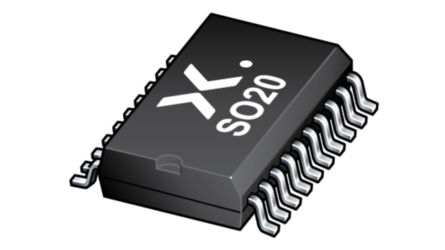
| Package Type | SO | |
| Maximum Supply Voltage | 6V | |
| Pin Count | 20 | |
| Minimum Operating Temperature | -40°C | |
| Maximum Operating Temperature | 125°C | |
| Height | 2.45mm | |
| Series | 74HC | |
| Standards/Approvals | No | |
| Length | 13mm | |
| Automotive Standard | No | |
| 選取全部 | ||
|---|---|---|
品牌 Nexperia | ||
Product Type Latch | ||
Logic Family 74HC | ||
Logic Function D Type | ||
Latch Mode Addressable | ||
Number of Bits 8 | ||
Output Type D Type Flip-Flop | ||
Polarity Non-Inverting | ||
Mount Type Surface | ||
Minimum Supply Voltage 2V | ||
Package Type SO | ||
Maximum Supply Voltage 6V | ||
Pin Count 20 | ||
Minimum Operating Temperature -40°C | ||
Maximum Operating Temperature 125°C | ||
Height 2.45mm | ||
Series 74HC | ||
Standards/Approvals No | ||
Length 13mm | ||
Automotive Standard No | ||
The 74HC273, 74HCT273 is an octal positive-edge triggered D-type flip-flop. The device features clock (CP) and master reset (MR) inputs. The outputs Qn will assume the state of their corresponding Dn inputs that meet the set-up and hold time requirements on the LOW-to-HIGH clock (CP) transition. A LOW on MR forces the outputs LOW independently of clock and data inputs. Inputs include clamp diodes. This enables the use of current limiting resistors to interface inputs to voltages in excess of VCC.
Mixed 5 V and 3.3 V applications
Improved signal integrity with integrated termination resistors
High noise immunity
Flow through pin out for easy layout
Wide supply voltage range
Low propagation delay
Overvoltage tolerant input options
Integrated source termination resistor options
Bus hold options
Key applications
Frequency division
Controlled delays
Interface between asynchronous and synchronous systems