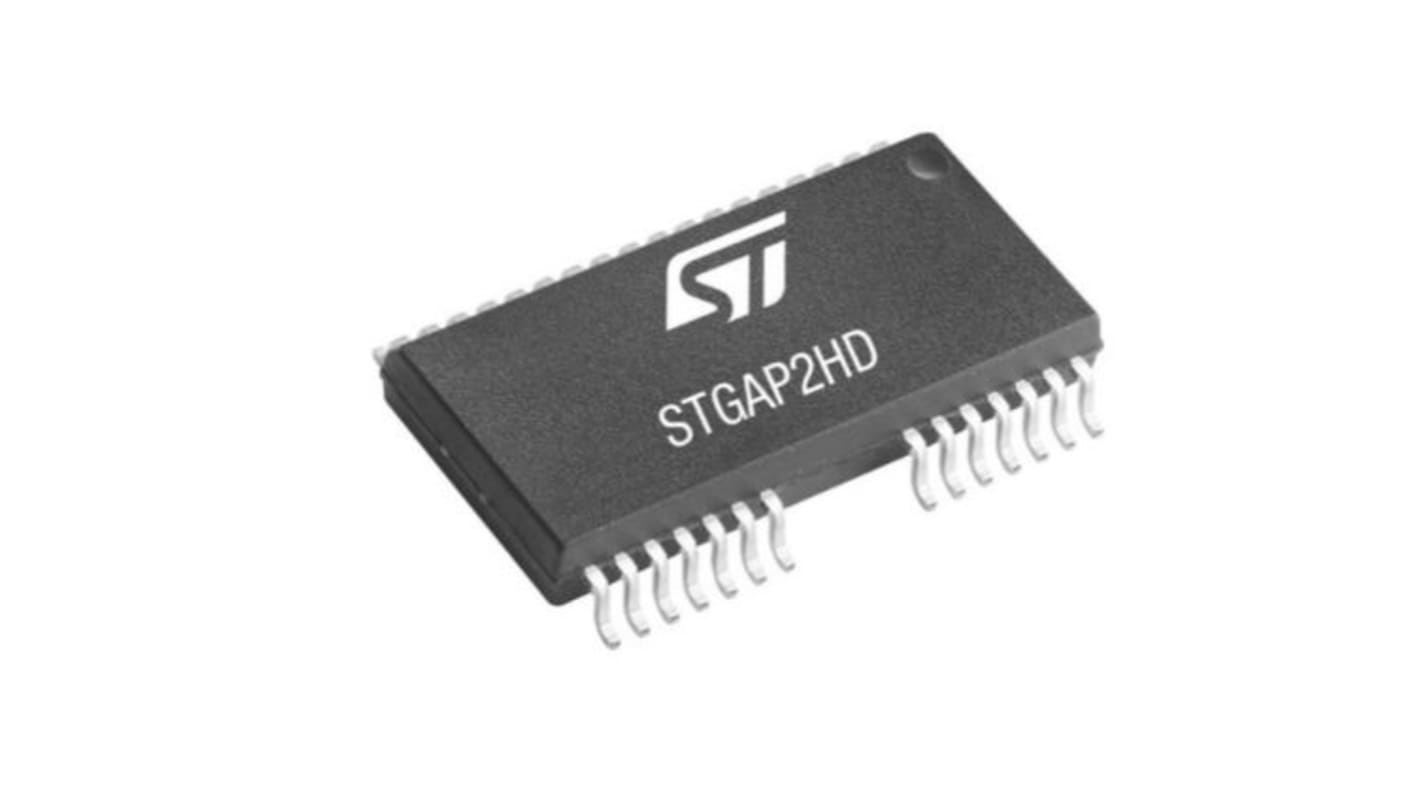
STMicroelectronics MOSFET Gate Driver, 4 A 36-Pin 5.5 V, SO-36W
- RS庫存編號:
- 239-5531
- 製造零件編號:
- STGAP2HDMTR
- 製造商:
- STMicroelectronics

此圖片僅供參考,請參閲產品詳細資訊及規格
可享批量折扣
小計(1 卷,共 1000 件)*
TWD106,800.00
(不含稅)
TWD112,140.00
(含稅)
訂單超過 $1,300.00 免費送貨
暫時缺貨
- 從 2026年12月16日 發貨
**需要更多嗎?**輸入您需要的數量,然後按一下「查看送貨日期」以查詢更多庫存和送貨詳細資訊。
單位 | 每單位 | 每卷* |
|---|---|---|
| 1000 - 1000 | TWD106.80 | TWD106,800.00 |
| 2000 + | TWD103.60 | TWD103,600.00 |
* 參考價格
- RS庫存編號:
- 239-5531
- 製造零件編號:
- STGAP2HDMTR
- 製造商:
- STMicroelectronics
規格
產品概覽和技術數據資料表
法例與合規
產品詳細資訊
透過選取一個或多個屬性來查找類似產品。
選取全部 | 屬性 | 值 |
|---|---|---|
| 品牌 | STMicroelectronics | |
| Product Type | MOSFET | |
| Output Current | 4A | |
| Pin Count | 36 | |
| Package Type | SO-36W | |
| Fall Time | 30ns | |
| Driver Type | MOSFET | |
| Minimum Supply Voltage | 3.1V | |
| Maximum Supply Voltage | 5.5V | |
| Minimum Operating Temperature | -40°C | |
| Maximum Operating Temperature | 125°C | |
| Standards/Approvals | No | |
| Series | STGAP | |
| Automotive Standard | No | |
| 選取全部 | ||
|---|---|---|
品牌 STMicroelectronics | ||
Product Type MOSFET | ||
Output Current 4A | ||
Pin Count 36 | ||
Package Type SO-36W | ||
Fall Time 30ns | ||
Driver Type MOSFET | ||
Minimum Supply Voltage 3.1V | ||
Maximum Supply Voltage 5.5V | ||
Minimum Operating Temperature -40°C | ||
Maximum Operating Temperature 125°C | ||
Standards/Approvals No | ||
Series STGAP | ||
Automotive Standard No | ||
The STMicroelectronics STGAP2HD is a dual gate driver which provides galvanic isolation between each gate driving channel and the low voltage control and interface circuitry. The gate driver is characterized by 4 A current capability and rail-to-rail outputs, making it suitable for mid and high power applications such as power conversion and industrial motor driver inverters. The separated output pins allow to independently optimize turn-on and turn-off by using dedicated gate resistors, while the Miller CLAMP function allows avoiding gate spikes during fast commutations in half-bridge topologies. The device integrates protection functions: dedicated SD and BRAKE pins are available, UVLO and thermal shutdown are included to easily design high reliability systems.
4 A Miller CLAMP
UVLO function
Configurable interlocking function
Dedicated SD and BRAKE pins
Gate driving voltage up to 26 V
3.3 V, 5 V TTL/CMOS inputs with hysteresis
Temperature shutdown protection
Standby function
6 kV galvanic isolation
Wide Body SO-36W
In half-bridge topologies the interlocking function prevents outputs from being high at the same time, avoiding shoot-through conditions in case of wrong logic input commands. The interlocking function can be disabled by a dedicated configuration pin, so to allow independent and parallel operation of the two channels. The input to output propagation delay results are contained within 75 ns, providing high PWM control accuracy. A standby mode is available in order to reduce idle power consumption.
相關連結
- STMicroelectronics STGAP2HDMTR MOSFET Gate Driver SO-36W
- STMicroelectronics MOSFET Gate Driver SO-36W
- STMicroelectronics STGAP2SICDTR MOSFET Gate Driver SO-36W
- STMicroelectronics STGAP4STR 2.5 A 36-Pin 7.2 V, SO-36W
- STMicroelectronics MOSFET Gate Driver 1 SO-8
- STMicroelectronics STGAP2SICS MOSFET Gate Driver 1 SO-8
- STMicroelectronics STGAP2HSCMTR MOSFET Gate Driver 1 SO-8
- STMicroelectronics STGAP2SICSNTR MOSFET Gate Driver 1 SO-8
