
小計(1 件)*
TWD5,552.00
(不含稅)
TWD5,829.60
(含稅)
訂單超過 $1,300.00 免費送貨
有庫存
- 加上 32 件從 2026年7月13日 起發貨
- 加上 18 件從 2026年9月03日 起發貨
- 加上 18 件從 2026年11月05日 起發貨
**需要更多嗎?**輸入您需要的數量,然後按一下「查看送貨日期」以查詢更多庫存和送貨詳細資訊。
單位 | 每單位 |
|---|---|
| 1 + | TWD5,552.00 |
* 參考價格
- RS庫存編號:
- 768-9039
- 製造零件編號:
- P0082
- 製造商:
- Terasic
規格
產品概覽和技術數據資料表
法例與合規
產品詳細資訊
透過選取一個或多個屬性來查找類似產品。
選取全部 | 屬性 | 值 |
|---|---|---|
| 品牌 | Terasic | |
| Kit Classification | Starter Kit | |
| Product Type | Communication & Wireless Development Tool | |
| For Use With | Cyclone IV | |
| Kit Name | Cyclone IV Deo-Nano | |
| Interface Type | USB | |
| Standards/Approvals | RoHS | |
| 選取全部 | ||
|---|---|---|
品牌 Terasic | ||
Kit Classification Starter Kit | ||
Product Type Communication & Wireless Development Tool | ||
For Use With Cyclone IV | ||
Kit Name Cyclone IV Deo-Nano | ||
Interface Type USB | ||
Standards/Approvals RoHS | ||
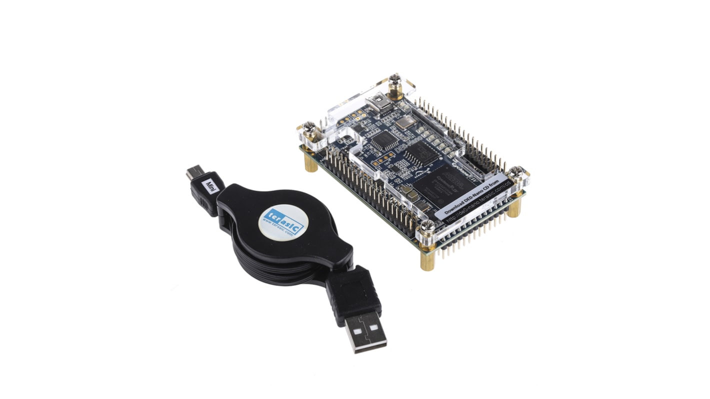
Cyclone IV DE0-Nano Starter Kit
The DE0-Nano board introduces a compact-sized FPGA development platform suited for prototyping circuit designs such as robots and "portable" projects. The board is designed, to be used in the simplest possible implementation targeting the Cyclone IV device with up to 22320 LEs.
The advantages of the DE0-Nano board include its size, weight and its ability to be reconfigured without carrying superfluous hardware. These features set it apart from other general purpose development boards.
Parallax has made all the design files for their 8-core Propeller microcontroller Open Source. Details of how to program the DE0-Nano as a Propeller together with all the necessary files can be found at:
http://www.parallax.com/microcontrollers/propeller-1-open-source
Altera Cyclone IV EP4CE22F17C6N FPGA, 22320 x Logic Elements, 594Kb memory, 66 x multipliers, 4 x PLLs, Maximum 153 x I/O pins
64 MB configuration Flash memory
50 MHz clock oscillator
32 MB SDRAM
2Kb I2C EEPROM
ADXL345 3-axis accelerometer
ADC128S022, 8-Channel, 12-bit A/D Converter, 50ksps to 200ksps
8 x green LEDs
2 x debounced push buttons
4 x dip switches
Power supply: Mini USB connector (5 V), Two GPIO header pins (5 V), 2-pin external power header (+3.6 to +5.7 V)
On-board USB-Blaster circuit for programming
Two 40-pin headers provide 72 x digital I/O pins
One 26-pin header provides 16 x digital I/O pins and 8 x analogue input pins
An FPGA is a semiconductor device consisting of a matrix of Configurable Logic Blocks (CLBs) connected through programmable interconnects. The user determines these interconnections by programming SRAM. A CLB can be simple (AND, OR gates, etc) or complex (a block of RAM). The FPGA allows changes to be made to a design even after the device is soldered into a PCB.
Supplied with
USB cable, System CD, Altera complete design suite free package, Quick Start Guide
相關連結
- Terasic SDI to HSMC SDI HSMC Board Adapter Board for Stratix IV GX FPGA Development Board P0039
- Terasic GPIO to HSMC/HSTC Adapter Board for DE3, DE2 P0024
- Altera FPGA Cyclone IV 28848 Cells 484-Pin FBGA
- Altera FPGA Cyclone IV GX 14400 Cells 169-Pin FBGA
- Altera FPGA EP4CGX15BF14C8N Cyclone IV GX 14400 Cells 169-Pin FBGA
- Altera FPGA Cyclone IV E 6272 Cells 276480 bit 392 Blocks, 256-Pin FBGA
- Altera FPGA Cyclone IV E 6272 Cells 276480 bit 392 Blocks, 144-Pin EQFP
- Altera FPGA EP4CE6F17C8LN Cyclone IV E 6272 Cells 276480 bit 392 Blocks, 256-Pin FBGA