Terasic SDI to HSMC SDI HSMC Board Adapter Board for Stratix IV GX FPGA Development Board P0039
- RS庫存編號:
- 768-9035
- 製造零件編號:
- P0039
- 製造商:
- Terasic

小計(1 件)*
TWD23,308.00
(不含稅)
TWD24,473.40
(含稅)
訂單超過 $1,300.00 免費送貨
暫時缺貨
- 從 2026年8月31日 發貨
**需要更多嗎?**輸入您需要的數量,然後按一下「查看送貨日期」以查詢更多庫存和送貨詳細資訊。
單位 | 每單位 |
|---|---|
| 1 + | TWD23,308.00 |
* 參考價格
- RS庫存編號:
- 768-9035
- 製造零件編號:
- P0039
- 製造商:
- Terasic
規格
產品概覽和技術數據資料表
法例與合規
產品詳細資訊
透過選取一個或多個屬性來查找類似產品。
選取全部 | 屬性 | 值 |
|---|---|---|
| 品牌 | Terasic | |
| Product Type | Communication & Wireless Development Tool | |
| Kit Classification | Adapter Board | |
| For Use With | Stratix IV GX FPGA Development Board | |
| Featured Device | SDI HSMC Board | |
| Kit Name | SDI to HSMC | |
| Interface Type | HSMC | |
| Standards/Approvals | AES3, SDI | |
| 選取全部 | ||
|---|---|---|
品牌 Terasic | ||
Product Type Communication & Wireless Development Tool | ||
Kit Classification Adapter Board | ||
For Use With Stratix IV GX FPGA Development Board | ||
Featured Device SDI HSMC Board | ||
Kit Name SDI to HSMC | ||
Interface Type HSMC | ||
Standards/Approvals AES3, SDI | ||
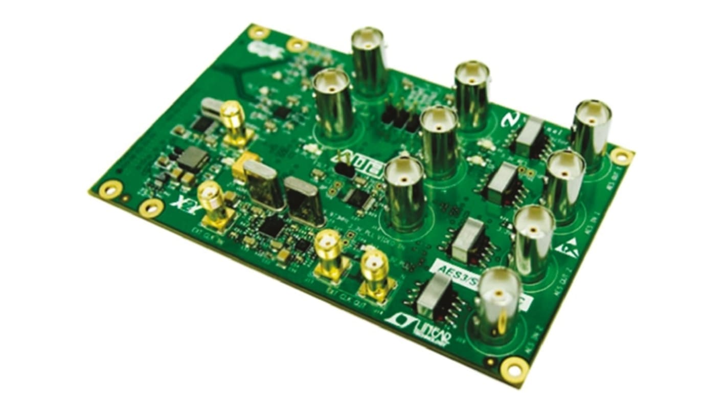
Terasic SDI HSMC Board
The Transceiver Serial Digital Interface (SDI) HSMC board provides a hardware platform for developing video broadcasting systems. It is intended to be used by customers to implement and design SDI and AES systems based on transceiver-based host boards with an HSMC interface. It can also be part of an openly sold Development Kit, or bundled with packages of software and IP cores.
2 x SDI transmit (TX) channels with SDI cable tri-speed drivers
2 x SDI receive (RX) channels with SDI cable equalizers
2 x 75Ω BNC SDI TX interfaces
2 x 75Ω BNC SDI RX interfaces
Adjustable 1.1 to 1.8V and standard 3.3V CMOS Input Signal Levels
2 x RS-422 transceivers for AES3 TX and AES3 RX channels
2 x 75Ω BNC AES3 RX interfaces
2 x 75Ω BNC AES3 TX interfaces
High frequency switching regulator for 12V to 5V power supply conversion
3 x linear regulators for 5V to 3.3V low noise power supply conversion
FDTIM analysis for power distribution network (PDN) decoupling
SDI multi-frequency VCXO femto clock video PLL
98.304MHz / 90.3168MHz / 122.88MHz / 112.896MHz voltage-controlled crystal oscillator (VCXO) based phase-locked loop (PLL)
LVPECL differential clock buffer with two differential outputs - HSMC and SMA
4 x digital audio isolation transformers
Multi-format video sync separator
HSMC connector for interface conversion, fully compatible with HSMC host boards
An FPGA is a semiconductor device consisting of a matrix of Configurable Logic Blocks (CLBs) connected through programmable interconnects. The user determines these interconnections by programming SRAM. A CLB can be simple (AND, OR gates, etc) or complex (a block of RAM). The FPGA allows changes to be made to a design even after the device is soldered into a PCB.
Supplied with
System CD ROM
相關連結
- Terasic GPIO to HSMC/HSTC Adapter Board for DE3, DE2 P0024
- Altera FPGA Cyclone IV GX 14400 Cells 169-Pin FBGA
- Altera FPGA EP4CGX15BF14C8N Cyclone IV GX 14400 Cells 169-Pin FBGA
- Digilent 410-319-1 FPGA Development Board for Makers and Hobbyists Development Board ADC1410 for DAC121S101
- Broadcom 1.9 V Red LED 1606 Surface HSMC HSMC-C120
- Digilent 410-370 Cora Z7: Zynq-7000 Development Board ADC1410 for FPGA Development, ARM Development
- Digilent 410-372 Adapter for use with APSoC Development Board, FPGA
- Broadcom 1.9 V Red LED 1606 Surface HSMC