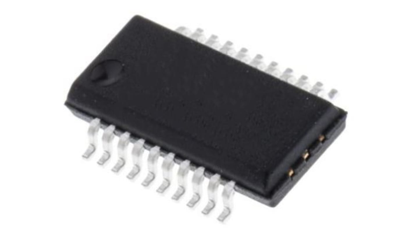
Renesas Electronics 49FCT3805QGI Clock Buffer 20-Pin QSOP
- RS庫存編號:
- 263-7892
- 製造零件編號:
- 49FCT3805QGI
- 製造商:
- Renesas Electronics

可享批量折扣
查看批量定價選項小計(1 包,共 5 件)*
TWD224.00
(不含稅)
TWD235.20
(含稅)
訂單超過 $1,300.00 免費送貨
有庫存
- 285 件準備從其他地點送貨
**需要更多嗎?**輸入您需要的數量,然後按一下「查看送貨日期」以查詢更多庫存和送貨詳細資訊。
單位 | 每單位 | 每包* |
|---|---|---|
| 5 - 5 | TWD44.80 | TWD224.00 |
| 10 - 20 | TWD40.00 | TWD200.00 |
| 25 - 105 | TWD37.80 | TWD189.00 |
| 110 - 270 | TWD32.00 | TWD160.00 |
| 275 + | TWD31.40 | TWD157.00 |
* 參考價格
- RS庫存編號:
- 263-7892
- 製造零件編號:
- 49FCT3805QGI
- 製造商:
- Renesas Electronics
規格
產品概覽和技術數據資料表
法例與合規
產品詳細資訊
透過選取一個或多個屬性來查找類似產品。
選取全部 | 屬性 | 值 |
|---|---|---|
| 品牌 | Renesas Electronics | |
| Product Type | Clock Buffer | |
| Maximum Propagation Delay Time | 5.2ns | |
| Mount Type | Surface | |
| Package Type | QSOP | |
| Pin Count | 20 | |
| Minimum Supply Voltage | 3.3V | |
| Maximum Supply Voltage | 5V | |
| Minimum Operating Temperature | -40°C | |
| Maximum Operating Temperature | 85°C | |
| Series | IDT49FCT3805 | |
| Length | 8.7mm | |
| Height | 1.47mm | |
| Standards/Approvals | RoHS | |
| 選取全部 | ||
|---|---|---|
品牌 Renesas Electronics | ||
Product Type Clock Buffer | ||
Maximum Propagation Delay Time 5.2ns | ||
Mount Type Surface | ||
Package Type QSOP | ||
Pin Count 20 | ||
Minimum Supply Voltage 3.3V | ||
Maximum Supply Voltage 5V | ||
Minimum Operating Temperature -40°C | ||
Maximum Operating Temperature 85°C | ||
Series IDT49FCT3805 | ||
Length 8.7mm | ||
Height 1.47mm | ||
Standards/Approvals RoHS | ||
- COO (Country of Origin):
- TW
The Renesas Electronics non-inverting clock driver built using Advanced dual metal CMOS technology. The device consists of two banks of drivers, each with a 1:5 fan out and its own output enable control. The device has a heartbeat monitor for diagnostics and PLL driving. Also is designed for high speed clock distribution where signal quality and skew are critical. The FCT3805 also allows single point-to point transmission line driving in applications such as address distribution, where one signal must be distributed to multiple receivers with low skew and high signal quality.
0.5 Micron CMOS Technology
Guaranteed low skew < 500ps
Very low duty cycle distortion < 1.0ns
Very low CMOS power levels
TTL compatible inputs and outputs
Inputs can be driven from 3.3V or 5V components
Two independent output banks with 3-state control
1:5 fan out per bank
相關連結
- Renesas Electronics 49FCT3805QGI Clock Buffer 20-Pin QSOP
- Renesas Electronics 49FCT3805PYGI Clock Buffer 20-Pin QSOP
- Renesas Electronics 49FCT3805AQGI Clock Buffer 20-Pin QSOP
- Renesas Electronics 49FCT3805AQGI8 Clock Driver, 20-Pin QSOP
- Renesas Electronics 49FCT3805QG8 Clock Driver, 20-Pin QSOP
- Renesas Electronics 49FCT3805AQG8 Clock Driver, 20-Pin QSOP
- Renesas Electronics 74FCT3807AQG8 Clock Driver, 20-Pin 10 QSOP
- Renesas Electronics 74FCT3807QGI8 Clock Driver, 20-Pin 10 QSOP