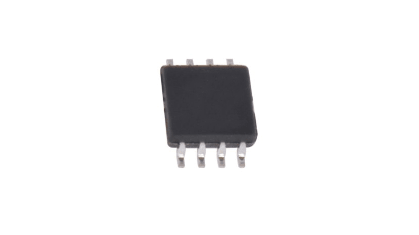
Renesas Electronics 5PB1102PGGK Clock Buffer 8-Pin TSSOP
- RS庫存編號:
- 254-4941
- 製造零件編號:
- 5PB1102PGGK
- 製造商:
- Renesas Electronics

此圖片僅供參考,請參閲產品詳細資訊及規格
可享批量折扣
小計(1 包,共 5 件)*
TWD294.00
(不含稅)
TWD308.70
(含稅)
訂單超過 $1,300.00 免費送貨
有庫存
- 加上 70 件從 2026年5月11日 起發貨
**需要更多嗎?**輸入您需要的數量,然後按一下「查看送貨日期」以查詢更多庫存和送貨詳細資訊。
單位 | 每單位 | 每包* |
|---|---|---|
| 5 - 5 | TWD58.80 | TWD294.00 |
| 10 - 20 | TWD52.60 | TWD263.00 |
| 25 - 45 | TWD50.00 | TWD250.00 |
| 50 - 90 | TWD49.20 | TWD246.00 |
| 95 + | TWD48.00 | TWD240.00 |
* 參考價格
- RS庫存編號:
- 254-4941
- 製造零件編號:
- 5PB1102PGGK
- 製造商:
- Renesas Electronics
規格
產品概覽和技術數據資料表
法例與合規
產品詳細資訊
透過選取一個或多個屬性來查找類似產品。
選取全部 | 屬性 | 值 |
|---|---|---|
| 品牌 | Renesas Electronics | |
| Product Type | Clock Buffer | |
| Maximum Input Frequency | 200MHz | |
| Maximum Propagation Delay Time | 2.5ns | |
| Mount Type | Surface | |
| Package Type | TSSOP | |
| Pin Count | 8 | |
| Minimum Supply Voltage | 1.71V | |
| Maximum Supply Voltage | 3.47V | |
| Minimum Operating Temperature | -40°C | |
| Maximum Operating Temperature | 105°C | |
| Length | 3.1mm | |
| Height | 1.2mm | |
| Standards/Approvals | RoHS | |
| Series | 5PB11xx | |
| Automotive Standard | No | |
| 選取全部 | ||
|---|---|---|
品牌 Renesas Electronics | ||
Product Type Clock Buffer | ||
Maximum Input Frequency 200MHz | ||
Maximum Propagation Delay Time 2.5ns | ||
Mount Type Surface | ||
Package Type TSSOP | ||
Pin Count 8 | ||
Minimum Supply Voltage 1.71V | ||
Maximum Supply Voltage 3.47V | ||
Minimum Operating Temperature -40°C | ||
Maximum Operating Temperature 105°C | ||
Length 3.1mm | ||
Height 1.2mm | ||
Standards/Approvals RoHS | ||
Series 5PB11xx | ||
Automotive Standard No | ||
The Renesas Electronics high-performance LVCMOS clock buffer has an additive phase jitter of 50 fs RMS. There are five different fan-out variations available that is 1:2 to 1:10. Its supports a synchronous glitch-free output enable (OE) function to eliminate any potential intermediate incorrect output clock cycles when enabling or disabling outputs. It can operate from a 1.8 V to 3.3 V supply.
High-performance 1:2, 1:4, 1:6, 1:8, 1:10 LVCMOS clock buffer
Very low pin-to-pin skew: < 50 ps
Very low additive jitter: < 50 fs
Supply voltage: 1.8 V to 3.3 V
3.3 V tolerant input clock
fMAX is 200 MHz
Integrated serial termination for 50 Ω channel
Packaged in 8-, 14-, 16-, 20-pin TSSOP and as small as 2 x 2 mm DFN and 3 x 3 mm VFQFPN packages
Industrial (-40°C to +85°C) and extended (-40°C to +105°C) temperature ranges
相關連結
- Renesas Electronics Clock Buffer 8-Pin TSSOP
- Renesas Electronics 5PB1104PGGK Clock Buffer 8-Pin TSSOP
- Renesas Electronics 5PB1104PGGI8 Clock Buffer 8-Pin TSSOP
- Renesas Electronics 2305-1DCGI8 Clock Buffer 8-Pin TSSOP
- Renesas Electronics Clock Buffer 48-Pin TSSOP
- Renesas Electronics Clock Buffer 20-Pin TSSOP
- Renesas Electronics 5PB1102CMGI8 Clock Buffer, 8-Pin TSSOP
- Renesas Electronics 9DB106BGLF Clock Buffer 28-Pin TSSOP
