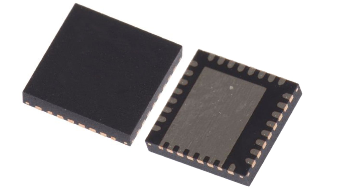
Renesas Electronics 9DBV0431AKILF Buffer 32-Pin QFN
- RS庫存編號:
- 249-4404
- 製造零件編號:
- 9DBV0431AKILF
- 製造商:
- Renesas Electronics

小計(1 托盤,共 490 件)*
TWD41,650.00
(不含稅)
TWD43,732.50
(含稅)
訂單超過 $1,300.00 免費送貨
暫時缺貨
- 從 2026年4月13日 發貨
**需要更多嗎?**輸入您需要的數量,然後按一下「查看送貨日期」以查詢更多庫存和送貨詳細資訊。
單位 | 每單位 | 每托盤* |
|---|---|---|
| 490 + | TWD85.00 | TWD41,650.00 |
* 參考價格
- RS庫存編號:
- 249-4404
- 製造零件編號:
- 9DBV0431AKILF
- 製造商:
- Renesas Electronics
規格
產品概覽和技術數據資料表
法例與合規
產品詳細資訊
透過選取一個或多個屬性來查找類似產品。
選取全部 | 屬性 | 值 |
|---|---|---|
| 品牌 | Renesas Electronics | |
| Number of Elements per Chip | 4 | |
| Maximum Supply Current | 4 mA | |
| Maximum Input Frequency | 137.5MHz | |
| Mounting Type | Surface Mount | |
| Package Type | QFN | |
| Pin Count | 32 | |
| 選取全部 | ||
|---|---|---|
品牌 Renesas Electronics | ||
Number of Elements per Chip 4 | ||
Maximum Supply Current 4 mA | ||
Maximum Input Frequency 137.5MHz | ||
Mounting Type Surface Mount | ||
Package Type QFN | ||
Pin Count 32 | ||
The Renesas Electronics 9DBV0431 is a 4-output very low power buffer for 100 MHz PCIe Gen1, Gen2 and Gen3 applications. It can also be used for 50M or 125M Ethernet Applications via software frequency selection. The device has 4 output enables for clock management.
1.8 V operation: minimal power consumption
OE# pins: support DIF power management
HCSL compatible differential input: can be driven by common clock sources
LP-HCSL differential clock outputs: reduced power and board space
Programmable slew rate for each output: allows tuning for various line lengths
Programmable output amplitude: allows tuning for various application environments
Pin/software selectable PLL bandwidth and PLL Bypass: minimize phase jitter for each application
Outputs blocked until PLL is locked: clean system start-up
Software selectable 50 MHz or 125 MHz PLL operation: useful for Ethernet applications
Configuration can be accomplished with strapping pins: SMBus interface not required for device control
3.3 V tolerant SMBus interface works with legacy controllers
For these non-cancellable (NC), and non-returnable (NR) products, Terms and Conditions apply.
相關連結
- Renesas Electronics 9DBV0431AKILF Buffer 32-Pin QFN
- Renesas Electronics 9DML0451AKILF Buffer 24-Pin QFN
- Renesas Electronics 5P83908NDGK Clock Buffer 20-Pin 20-pin QFN
- Renesas Electronics 9DBV0441AKILF Buffer 32-Pin VFQFPN
- Renesas Electronics 9DBV0441AKLF Clock Buffer 32-Pin VFQFPN
- Renesas Electronics 9DML4493ANLGI Clock Buffer 32-Pin VFQFPN
- onsemi NB7L572MNG PLL Clock Buffer 32-Pin QFN
- Renesas Electronics 5PB1110PGGI Clock Buffer 20-Pin TSSOP