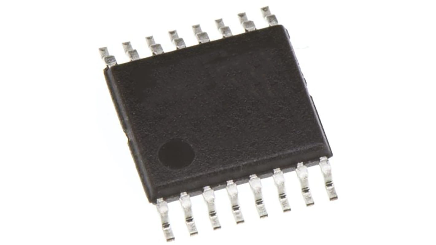
Infineon CY2309SXI-1H PLL Clock Buffer 16-Pin TSSOP
- RS庫存編號:
- 194-9032
- 製造零件編號:
- CY2309SXI-1H
- 製造商:
- Infineon

此圖片僅供參考,請參閲產品詳細資訊及規格
可享批量折扣
小計(1 件)*
TWD593.00
(不含稅)
TWD622.65
(含稅)
訂單超過 $1,300.00 免費送貨
最後的 RS 庫存
- 最終 40 個,準備發貨
單位 | 每單位 |
|---|---|
| 1 - 11 | TWD593.00 |
| 12 - 23 | TWD577.00 |
| 24 + | TWD570.00 |
* 參考價格
- RS庫存編號:
- 194-9032
- 製造零件編號:
- CY2309SXI-1H
- 製造商:
- Infineon
規格
產品概覽和技術數據資料表
法例與合規
產品詳細資訊
透過選取一個或多個屬性來查找類似產品。
選取全部 | 屬性 | 值 |
|---|---|---|
| 品牌 | Infineon | |
| Product Type | PLL Clock Buffer | |
| Maximum Input Frequency | 133MHz | |
| Package Type | TSSOP | |
| Pin Count | 16 | |
| Minimum Operating Temperature | -40°C | |
| Maximum Operating Temperature | 85°C | |
| Width | 4.5 mm | |
| Height | 0.95mm | |
| Length | 5.1mm | |
| 選取全部 | ||
|---|---|---|
品牌 Infineon | ||
Product Type PLL Clock Buffer | ||
Maximum Input Frequency 133MHz | ||
Package Type TSSOP | ||
Pin Count 16 | ||
Minimum Operating Temperature -40°C | ||
Maximum Operating Temperature 85°C | ||
Width 4.5 mm | ||
Height 0.95mm | ||
Length 5.1mm | ||
The CY2309 is a low-cost 3.3 V zero delay buffer designed to distribute high speed clocks and is available in a 16-pin SOIC or TSSOP package. The CY2305 is an 8-pin version of the CY2309. It accepts one reference input, and drives out five low skew clocks. The -1H versions of each device operate at up to 100-/133 MHz frequencies, and have higher drive than the -1 devices. All parts have on-chip PLLs which lock to an input clock on the REF pin. The PLL feedback is on-chip and is obtained from the CLKOUT pad. The CY2309 has two banks of four outputs each, which can be controlled by the select inputs. If all output clocks are not required, Bank B can be three-stated. The select inputs also allow the input clock to be directly applied to the outputs for chip and system testing purposes. The CY2305 and CY2309 PLLs enter a power-down mode when there are no rising edges on the REF input. In this state, the outputs are three-stated and the PLL is turned off, resulting in less than 25.0 μA current draw for these parts.
相關連結
- Infineon CY2309SXI-1H PLL Clock Buffer 16-Pin TSSOP
- Infineon CY2308ZXI-1H PLL Clock Buffer 16-Pin TSSOP
- Infineon CY2308SXI-1 PLL Clock Buffer 16-Pin SOIC
- Texas Instruments PLL Clock Buffer 8-Pin TSSOP
- Infineon CY2305SXI-1H Clock Buffer 8-Pin SOIC
- Texas Instruments CDCLVC1102PW PLL Clock Buffer 8-Pin TSSOP
- Texas Instruments CDCLVC1104PW PLL Clock Buffer 8-Pin TSSOP
- Renesas Electronics 9DB106BGILFT PLL Clock Buffer 28-Pin TSSOP-28
