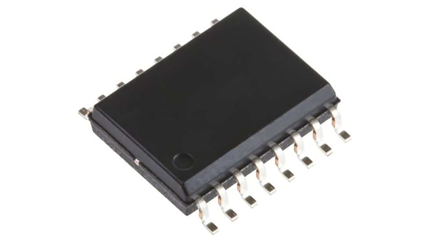
Infineon CY2308SXI-1 PLL Clock Buffer 16-Pin SOIC
- RS庫存編號:
- 194-9014
- 製造零件編號:
- CY2308SXI-1
- 製造商:
- Infineon

此圖片僅供參考,請參閲產品詳細資訊及規格
可享批量折扣
小計(1 件)*
TWD404.00
(不含稅)
TWD424.20
(含稅)
訂單超過 $1,300.00 免費送貨
最後的 RS 庫存
- 最終 3 個,準備發貨
單位 | 每單位 |
|---|---|
| 1 - 11 | TWD404.00 |
| 12 - 23 | TWD395.00 |
| 24 + | TWD370.00 |
* 參考價格
- RS庫存編號:
- 194-9014
- 製造零件編號:
- CY2308SXI-1
- 製造商:
- Infineon
規格
產品概覽和技術數據資料表
法例與合規
產品詳細資訊
透過選取一個或多個屬性來查找類似產品。
選取全部 | 屬性 | 值 |
|---|---|---|
| 品牌 | Infineon | |
| Product Type | PLL Clock Buffer | |
| Maximum Input Frequency | 133.3MHz | |
| Package Type | SOIC | |
| Pin Count | 16 | |
| Minimum Operating Temperature | -40°C | |
| Maximum Operating Temperature | 85°C | |
| Width | 3.98 mm | |
| Length | 9.98mm | |
| Height | 1.47mm | |
| 選取全部 | ||
|---|---|---|
品牌 Infineon | ||
Product Type PLL Clock Buffer | ||
Maximum Input Frequency 133.3MHz | ||
Package Type SOIC | ||
Pin Count 16 | ||
Minimum Operating Temperature -40°C | ||
Maximum Operating Temperature 85°C | ||
Width 3.98 mm | ||
Length 9.98mm | ||
Height 1.47mm | ||
The CY2308 is a 3.3 V Zero Delay Buffer designed to distribute high speed clocks in PC, workstation, datacom, telecom, and other high performance applications. The part has an on-chip PLL that locks to an input clock presented on the REF pin. The PLL feedback is driven from external FBK pin, so user has flexibility to choose any one of the outputs as feedback input and connect it to FBK pin. The input-to-output skew is less than 250 ps and output-to-output skew is less than 200 ps. The CY2308 has two banks of four outputs each that is controlled by the select inputs as shown in the table Select Input Decoding on page 3. If all output clocks are not required, Bank B is three-stated. The input clock is directly applied to the output for chip and system testing purposes by the select inputs. The CY2308 PLL enters a power down state when there are no rising edges on the REF input. In this mode, all outputs are three-stated and the PLL is turned off resulting in less than 25 μA of current draw.
相關連結
- Infineon CY2308SXI-1 PLL Clock Buffer 16-Pin SOIC
- Infineon CY2302SXI-1 PLL Clock Buffer 8-Pin SOIC
- Infineon CY2309SXI-1H PLL Clock Buffer 16-Pin TSSOP
- Infineon CY2308ZXI-1H PLL Clock Buffer 16-Pin TSSOP
- onsemi PLL Clock Buffer 8-Pin SOIC
- onsemi MC100EL11DG PLL Clock Buffer 8-Pin SOIC
- onsemi MC100LVEP11DG PLL Clock Buffer 8-Pin SOIC
- onsemi MC100LVEL11DG PLL Clock Buffer 8-Pin SOIC
