Alliance Memory SDRAM 1 GB Surface, 84-Pin 16 bit FBGA
- RS庫存編號:
- 230-8437P
- 製造零件編號:
- AS4C64M16D2A-25BIN
- 製造商:
- Alliance Memory

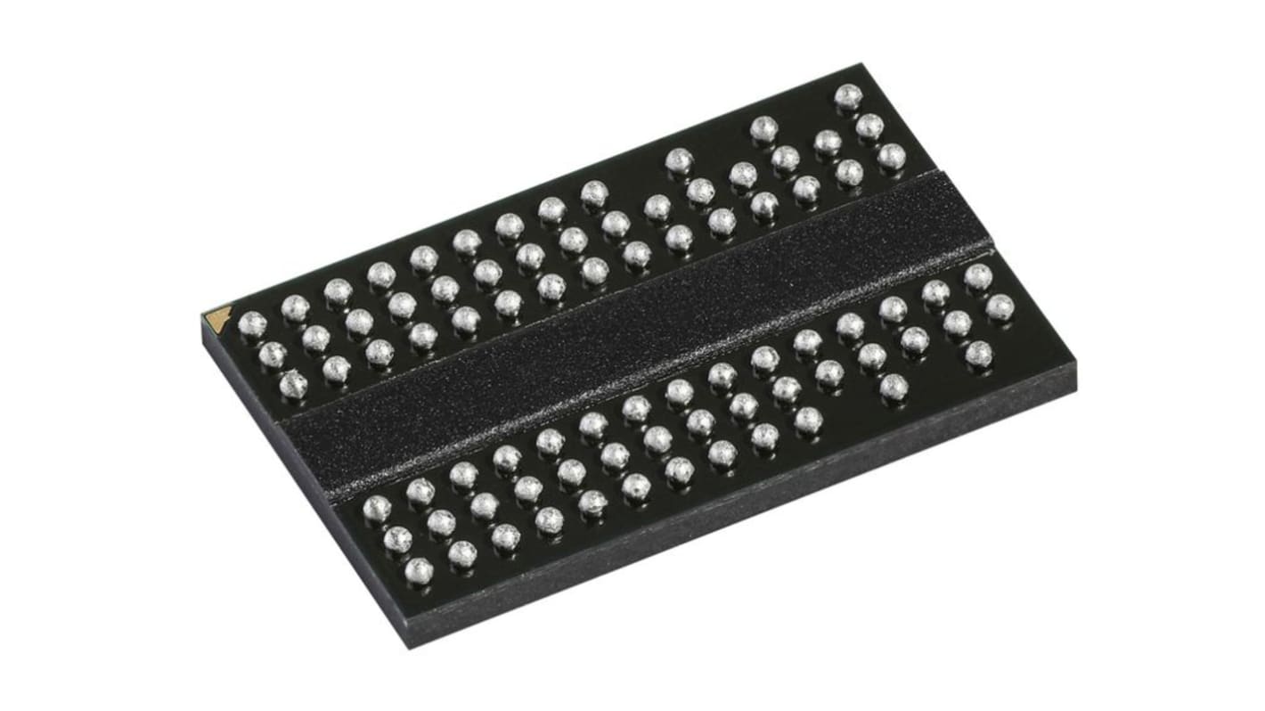
此圖片僅供參考,請參閲產品詳細資訊及規格
可享批量折扣
小計 10 件 (以盤裝提供)*
TWD1,850.00
(不含稅)
TWD1,942.50
(含稅)
訂單超過 $1,300.00 免費送貨
有庫存
- 加上 2 件從 2026年3月23日 起發貨
**需要更多嗎?**輸入您需要的數量,然後按一下「查看送貨日期」以查詢更多庫存和送貨詳細資訊。
單位 | 每單位 |
|---|---|
| 10 - 24 | TWD185.00 |
| 25 - 49 | TWD179.00 |
| 50 - 99 | TWD176.00 |
| 100 + | TWD172.00 |
* 參考價格
- RS庫存編號:
- 230-8437P
- 製造零件編號:
- AS4C64M16D2A-25BIN
- 製造商:
- Alliance Memory
規格
產品概覽和技術數據資料表
法例與合規
產品詳細資訊
透過選取一個或多個屬性來查找類似產品。
選取全部 | 屬性 | 值 |
|---|---|---|
| 品牌 | Alliance Memory | |
| Memory Size | 1GB | |
| Product Type | SDRAM | |
| Organisation | 64M x 16 | |
| Data Bus Width | 16bit | |
| Address Bus Width | 13bit | |
| Maximum Clock Frequency | 400MHz | |
| Number of Bits per Word | 16 | |
| Maximum Random Access Time | 0.4ns | |
| Mount Type | Surface | |
| Package Type | FBGA | |
| Minimum Operating Temperature | -40°C | |
| Pin Count | 84 | |
| Maximum Operating Temperature | 95°C | |
| Height | 1.2mm | |
| Standards/Approvals | RoHS | |
| Series | AS4C64M16D2A | |
| Width | 12.5 mm | |
| Length | 8.1mm | |
| Maximum Supply Voltage | 1.9V | |
| Minimum Supply Voltage | 1.7V | |
| Automotive Standard | No | |
| 選取全部 | ||
|---|---|---|
品牌 Alliance Memory | ||
Memory Size 1GB | ||
Product Type SDRAM | ||
Organisation 64M x 16 | ||
Data Bus Width 16bit | ||
Address Bus Width 13bit | ||
Maximum Clock Frequency 400MHz | ||
Number of Bits per Word 16 | ||
Maximum Random Access Time 0.4ns | ||
Mount Type Surface | ||
Package Type FBGA | ||
Minimum Operating Temperature -40°C | ||
Pin Count 84 | ||
Maximum Operating Temperature 95°C | ||
Height 1.2mm | ||
Standards/Approvals RoHS | ||
Series AS4C64M16D2A | ||
Width 12.5 mm | ||
Length 8.1mm | ||
Maximum Supply Voltage 1.9V | ||
Minimum Supply Voltage 1.7V | ||
Automotive Standard No | ||
The Alliance Memory AS4C64M16D2A is a high-speed CMOS Double-Data-Rate-Two (DDR2), synchronous dynamic random- access memory (SDRAM) containing 1024 Mbits in a 16-bit wide data I/Os. It is internally configured as a 8-bank DRAM, 8 banks x 8Mb addresses x 16 I/Os. The device is designed to comply with DDR2 DRAM key features such as posted CAS# with additive latency, Write latency = Read latency -1, Off-Chip Driver (OCD) impedance adjustment, and On Die Termination(ODT).
Supports JEDEC clock jitter specification
Fully synchronous operation
Fast clock rate: 400 MHz
Differential Clock, CK & CK#
Bidirectional single/differential data strobe DQS & DQS#
8 internal banks for concurrent operation
4-bit prefetch architecture
Inte