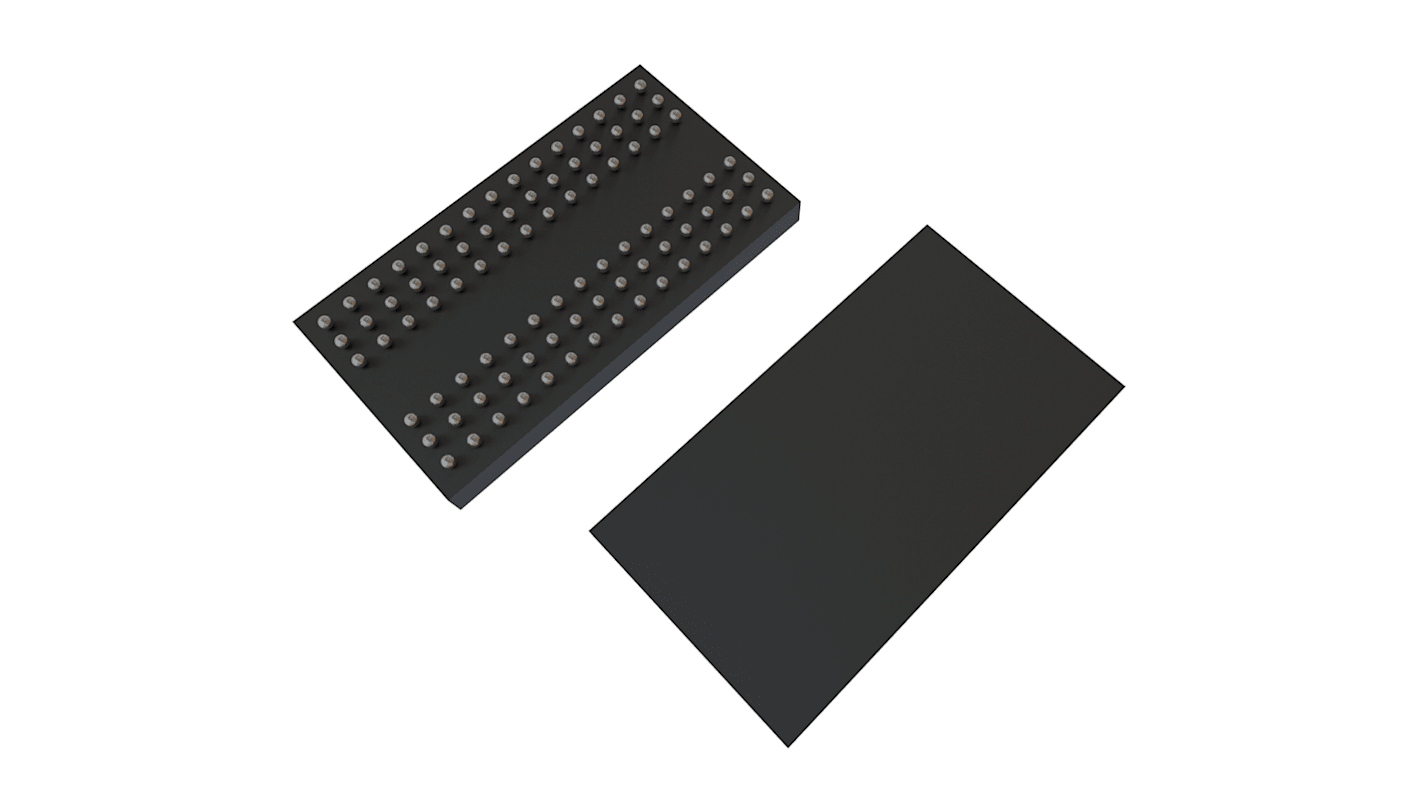
Winbond W972GG8KB25I, SDRAM 2Gbit Surface Mount, 60-Pin WBGA
- RS庫存編號:
- 188-2585
- 製造零件編號:
- W972GG8KB25I
- 製造商:
- Winbond

不可供應
RS 不再對此產品進貨。
- RS庫存編號:
- 188-2585
- 製造零件編號:
- W972GG8KB25I
- 製造商:
- Winbond
規格
產品概覽和技術數據資料表
法例與合規
產品詳細資訊
透過選取一個或多個屬性來查找類似產品。
選取全部 | 屬性 | 值 |
|---|---|---|
| 品牌 | Winbond | |
| Memory Size | 2Gbit | |
| Organisation | 256M x 8 bit | |
| Number of Bits per Word | 8bit | |
| Number of Words | 256M | |
| Mounting Type | Surface Mount | |
| Package Type | WBGA | |
| Pin Count | 60 | |
| Dimensions | 12.6 x 8.1 x 0.6mm | |
| Height | 0.6mm | |
| Length | 12.6mm | |
| Width | 8.1mm | |
| Maximum Operating Supply Voltage | 1.9 V | |
| Maximum Operating Temperature | +95 °C | |
| Minimum Operating Supply Voltage | 1.7 V | |
| Minimum Operating Temperature | -40 °C | |
| 選取全部 | ||
|---|---|---|
品牌 Winbond | ||
Memory Size 2Gbit | ||
Organisation 256M x 8 bit | ||
Number of Bits per Word 8bit | ||
Number of Words 256M | ||
Mounting Type Surface Mount | ||
Package Type WBGA | ||
Pin Count 60 | ||
Dimensions 12.6 x 8.1 x 0.6mm | ||
Height 0.6mm | ||
Length 12.6mm | ||
Width 8.1mm | ||
Maximum Operating Supply Voltage 1.9 V | ||
Maximum Operating Temperature +95 °C | ||
Minimum Operating Supply Voltage 1.7 V | ||
Minimum Operating Temperature -40 °C | ||
Power Supply: VDD, VDDQ = 1.8 V ± 0.1 V
Double Data Rate architecture: two data transfers per clock cycle
CAS Latency: 3, 4, 5, 6 and 7
Burst Length: 4 and 8
Bi-directional, differential data strobes (DQS and DQS) are transmitted / received with data
Edge-aligned with Read data and center-aligned with Write data
DLL aligns DQ and DQS transitions with clock
Differential clock inputs (CLK and CLK)
Data masks (DM) for write data
Commands entered on each positive CLK edge, data and data mask are referenced to both edges of DQS
Posted CAS programmable additive latency supported to make command and data bus efficiency
Read Latency = Additive Latency plus CAS Latency (RL = AL + CL)
Off-Chip-Driver impedance adjustment (OCD) and On-Die-Termination (ODT) for better signal quality
Auto-precharge operation for read and write bursts
Auto Refresh and Self Refresh modes
Precharged Power Down and Active Power Down
Write Data Mask
Write Latency = Read Latency - 1 (WL = RL - 1)
Interface: SSTL_18
Packaged in WBGA 60 Ball (8x12.5 mm2), using Lead free materials.