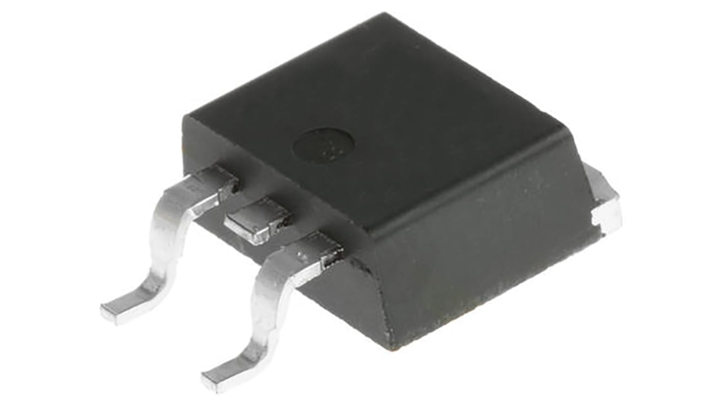
N-Channel MOSFET, 18 A, 200 V, 3-Pin D2PAK Infineon IRF640NSTRLPBF
- RS庫存編號:
- 831-2853P
- 製造零件編號:
- IRF640NSTRLPBF
- 製造商:
- Infineon

可享批量折扣
單價 個 (以每卷裝提供)**. Quantities below 150 on continuous strip
TWD31.90
(不含稅)
TWD33.50
(含稅)
1320 現貨庫存,可於6工作日發貨。*
* 交貨日期可能會根據您選擇的數量和交貨地址而變更。
訂單金額滿 TWD2,857.00 (未稅) 即可享受 免費 送貨服務
單位 | 每單位 |
|---|---|
| 200 + | TWD29.50 |
** 參考價格
- RS庫存編號:
- 831-2853P
- 製造零件編號:
- IRF640NSTRLPBF
- 製造商:
- Infineon
- COO (Country of Origin):
- KR
N-Channel Power MOSFET 150V to 600V, Infineon
Infineon's range of discrete HEXFET® power MOSFETs includes N-channel devices in surface mount and leaded packages and form factors that can address almost any board layout and thermal design challenge. Across the range benchmark on resistance drives down conduction losses, allowing designers to deliver optimum system efficiency.
Infineon HEXFET Series MOSFET, 18A Maximum Continuous Drain Current, 150W Maximum Power Dissipation - IRF640NSTRLPBF
This MOSFET is essential for efficient power management across various applications, controlling electrical current flow in circuits to ensure performance and reliability. Its robust specifications make it particularly suitable for automation and electronic systems in contemporary electronics.
Features & Benefits
• N-channel configuration supports enhancement mode operation
• Maximum continuous drain current of 18A
• Peak drain-source voltage of 200V for diverse applications
• D2PAK package designed for surface mount convenience
• Low Rds(on) of 150mΩ reduces energy loss during operation
• High maximum operating temperature of +175°C for various environments
• Maximum continuous drain current of 18A
• Peak drain-source voltage of 200V for diverse applications
• D2PAK package designed for surface mount convenience
• Low Rds(on) of 150mΩ reduces energy loss during operation
• High maximum operating temperature of +175°C for various environments
Applications
• Power management in automotive electronics
• Industrial power supplies for automation systems
• Motor control across different sectors
• Renewable energy systems for energy conversion
• High-frequency power inverter designs
• Industrial power supplies for automation systems
• Motor control across different sectors
• Renewable energy systems for energy conversion
• High-frequency power inverter designs
What is the maximum drain-source voltage?
The maximum drain-source voltage rating is 200V, providing flexibility for high-voltage applications.
How is heat dissipation managed during operation?
This MOSFET offers a power dissipation capability of 150W, and its package design promotes effective heat management under high loads.
What are the implications of the gate threshold voltage range?
With a maximum gate threshold voltage of 4V and a minimum of 2V, it offers engineers a versatile range for switching applications.
Can this component be used in parallel configurations?
Yes, it can be easily paralleled due to its low on-resistance, making it suitable for high current applications.
How should it be soldered for optimal performance?
The soldering temperature should not exceed 300°C for 10 seconds to ensure proper installation without damaging the MOSFET.
For products that are Customized and under Non-cancellable & Non-returnable, Sales & Conditions apply.
MOSFET Transistors, Infineon
Infineon offers a large and comprehensive portfolio of MOSFET devices which includes the CoolMOS, OptiMOS and StrongIRFET families. They deliver best-in-class performance to bring more efficiency, power density and cost effectiveness. Designs requiring high quality and enhanced protection features benefit from AEC-Q101 industry standards Automotive qualified MOSFETs.
屬性 | 值 |
|---|---|
| Channel Type | N |
| Maximum Continuous Drain Current | 18 A |
| Maximum Drain Source Voltage | 200 V |
| Package Type | D2PAK (TO-263) |
| Series | HEXFET |
| Mounting Type | Surface Mount |
| Pin Count | 3 |
| Maximum Drain Source Resistance | 150 mΩ |
| Channel Mode | Enhancement |
| Maximum Gate Threshold Voltage | 4V |
| Minimum Gate Threshold Voltage | 2V |
| Maximum Power Dissipation | 150 W |
| Transistor Configuration | Single |
| Maximum Gate Source Voltage | -20 V, +20 V |
| Transistor Material | Si |
| Width | 9.65mm |
| Maximum Operating Temperature | +175 °C |
| Typical Gate Charge @ Vgs | 67 nC @ 10 V |
| Length | 10.67mm |
| Number of Elements per Chip | 1 |
| Height | 4.83mm |
| Minimum Operating Temperature | -55 °C |
| Forward Diode Voltage | 1.3V |