服務
Ideas and Advice
折扣優惠
包裹追蹤
登入
主目錄
製造零件編號
最近搜索
Automation & Control Gear
Cables & Wires
Enclosures & Server Racks
Fuses & Circuit Breakers
HVAC, Fans & Thermal Management
Lighting
Relays & Signal Conditioning
Switches
Batteries & Chargers
Connectors
Displays & Optoelectronics
ESD Control, Cleanroom & PCB Prototyping
Passive Components
Power Supplies & Transformers
Raspberry Pi, Arduino, ROCK, STEM Education & Development Tools
Semiconductors
Access, Storage & Material Handling
Adhesives, Sealants & Tapes
Bearings & Seals
Engineering Materials & Industrial Hardware
Fasteners & Fixings
Hand Tools
Mechanical Power Transmission
Plumbing & Pipeline
Pneumatics & Hydraulics
Power Tools, Soldering & Welding
Computing & Peripherals
Facilities Cleaning & Maintenance
Office Supplies
Personal Protective Equipment & Workwear
Security & Ironmongery
Site Safety
Test & Measurement
Semiconductors
Discrete Semiconductors
MOSFETs
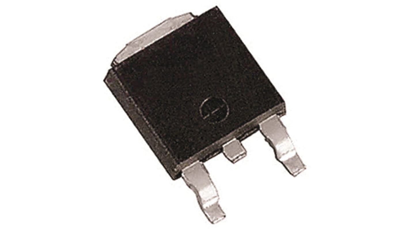
N-Channel MOSFET, 55 A, 100 V, 3-Pin DPAK Toshiba TK55S10N1
RS庫存編號:
171-2475
製造零件編號:
TK55S10N1
製造商:
Toshiba
查看所有MOSFETs
15 現貨庫存,可於6工作日發貨。
Add to Basket
單位
添加到購物車
即時庫存查詢
添加到收藏夾
單價(不含稅) 個 (每包:5個)
TWD57.20
(不含稅)
TWD60.06
(含稅)
單位
每單位
每包*
5 - 495
TWD57.20
TWD286.00
500 - 995
TWD55.80
TWD279.00
1000 +
TWD54.80
TWD274.00
* 參考價格
RS庫存編號:
171-2475
製造零件編號:
TK55S10N1
製造商:
Toshiba
產品概覽和技術數據資料表
法例與合規
產品詳細資訊
規格
Datasheet
ESD Control Selection Guide V1
豁免
符合聲明
COO (Country of Origin):
JP
Automotive
Switching Voltage Regulators
Motor Drivers
Low drain-source on-resistance: RDS(ON) = 5.5 mΩ (typ.) (VGS = 10 V)
Low leakage current: IDSS = 10 μA (max) (VDS = 100 V)
Enhancement mode: Vth = 2.0 to 4.0 V (VDS = 10 V, ID = 0.5 mA)
For products that are Customized and under Non-cancellable & Non-returnable, Sales & Conditions apply.
屬性
值
Channel Type
N
Maximum Continuous Drain Current
55 A
Maximum Drain Source Voltage
100 V
Package Type
DPAK (TO-252)
Mounting Type
Surface Mount
Pin Count
3
Maximum Drain Source Resistance
6.5 mΩ
Channel Mode
Enhancement
Maximum Gate Threshold Voltage
4V
Minimum Gate Threshold Voltage
2V
Maximum Power Dissipation
157 W
Transistor Configuration
Single
Maximum Gate Source Voltage
±20 V
Typical Gate Charge @ Vgs
49 nC @ 10 V
Length
6.5mm
Maximum Operating Temperature
+175 °C
Number of Elements per Chip
1
Width
7mm
Height
2.3mm
Forward Diode Voltage
1.2V
Automotive Standard
AEC-Q101