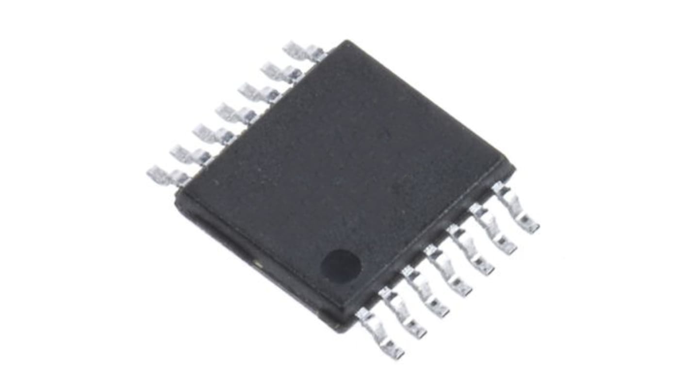
onsemi MC74VHC00DTG, Quad 2-Input NAND Logic Gate, 14-Pin TSSOP
- RS庫存編號:
- 186-8599P
- 製造零件編號:
- MC74VHC00DTG
- 製造商:
- onsemi

可享批量折扣
小計 125 件 (以管提供)*
TWD1,212.50
(不含稅)
TWD1,272.50
(含稅)
訂單超過 $1,300.00 免費送貨
有庫存
- 25 件準備從其他地點送貨
**需要更多嗎?**輸入您需要的數量,然後按一下「查看送貨日期」以查詢更多庫存和送貨詳細資訊。
單位 | 每單位 |
|---|---|
| 125 + | TWD9.70 |
* 參考價格
- RS庫存編號:
- 186-8599P
- 製造零件編號:
- MC74VHC00DTG
- 製造商:
- onsemi
規格
產品概覽和技術數據資料表
法例與合規
產品詳細資訊
透過選取一個或多個屬性來查找類似產品。
選取全部 | 屬性 | 值 |
|---|---|---|
| 品牌 | onsemi | |
| Logic Function | NAND | |
| Mounting Type | Surface Mount | |
| Number of Elements | 4 | |
| Number of Inputs per Gate | 2 | |
| Package Type | TSSOP | |
| Pin Count | 14 | |
| Logic Family | VHC | |
| Input Type | CMOS | |
| Maximum Operating Supply Voltage | 5.5 V | |
| Maximum High Level Output Current | -24mA | |
| Maximum Propagation Delay Time @ Maximum CL | 14.5 ns @ 50 pF | |
| Minimum Operating Supply Voltage | 2 V | |
| Maximum Low Level Output Current | 24mA | |
| Minimum Operating Temperature | -55 °C | |
| Dimensions | 5.1 x 4.5 x 1.05mm | |
| Maximum Operating Temperature | +125 °C | |
| Output Type | Bipolar Schottky TTL | |
| Propagation Delay Test Condition | 50pF | |
| Width | 4.5mm | |
| Height | 1.05mm | |
| Length | 5.1mm | |
| 選取全部 | ||
|---|---|---|
品牌 onsemi | ||
Logic Function NAND | ||
Mounting Type Surface Mount | ||
Number of Elements 4 | ||
Number of Inputs per Gate 2 | ||
Package Type TSSOP | ||
Pin Count 14 | ||
Logic Family VHC | ||
Input Type CMOS | ||
Maximum Operating Supply Voltage 5.5 V | ||
Maximum High Level Output Current -24mA | ||
Maximum Propagation Delay Time @ Maximum CL 14.5 ns @ 50 pF | ||
Minimum Operating Supply Voltage 2 V | ||
Maximum Low Level Output Current 24mA | ||
Minimum Operating Temperature -55 °C | ||
Dimensions 5.1 x 4.5 x 1.05mm | ||
Maximum Operating Temperature +125 °C | ||
Output Type Bipolar Schottky TTL | ||
Propagation Delay Test Condition 50pF | ||
Width 4.5mm | ||
Height 1.05mm | ||
Length 5.1mm | ||
The MC74VHC00 is an advanced high speed CMOS 2-input NAND gate fabricated with silicon gate CMOS technology. It achieves high speed operation similar to equivalent Bipolar Schottky TTL while maintaining CMOS low power dissipation. The internal circuit is composed of three stages, including a buffer output which provides high noise immunity and stable output. The inputs tolerate voltages up to 7V, allowing the interface of 5V systems to 3V systems.
High Speed: tPD = 3.7ns (Typ) at VCC = 5V
Low Power Dissipation: ICC = 2μA (Max) at TA = 25 C
High Noise Immunity: VNIH = VNIL = 28% VCC
Power Down Protection Provided on Inputs
Balanced Propagation Delays
Designed for 2V to 5.5V Operating Range
Low Noise: VOLP = 0.8V (Max)
Pin and Function Compatible with Other Standard Logic Families
Latchup Performance Exceeds 300mA
ESD Performance: HBM > 2000V, Machine Model > 200V
Chip Complexity: 32 FETs or 8 Equivalent Gates