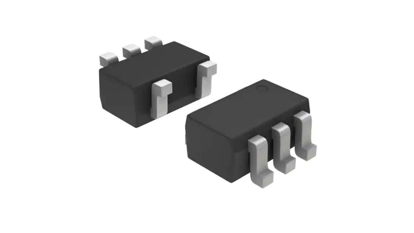
onsemi, 1 1-Input AND Logic Gate, 5-Pin SOT-353
- RS庫存編號:
- 184-4240
- 製造零件編號:
- M74VHC1GT08DFT2G
- 製造商:
- onsemi

此圖片僅供參考,請參閲產品詳細資訊及規格
暫時無法供應
我們無法確定此產品何時有貨,RS 預計將其從我們的產品目錄中移除。
- RS庫存編號:
- 184-4240
- 製造零件編號:
- M74VHC1GT08DFT2G
- 製造商:
- onsemi
規格
產品概覽和技術數據資料表
法例與合規
產品詳細資訊
透過選取一個或多個屬性來查找類似產品。
選取全部 | 屬性 | 值 |
|---|---|---|
| 品牌 | onsemi | |
| Logic Function | AND | |
| Product Type | Logic Gate | |
| Mount Type | Surface | |
| Number of Elements | 1 | |
| Number of Inputs per Gate | 1 | |
| Package Type | SOT-353 | |
| Pin Count | 5 | |
| Logic Family | 74VHC | |
| Input Type | TTL, CMOS | |
| Maximum Propagation Delay Time @ CL | 11ns | |
| Minimum Operating Temperature | -55°C | |
| Maximum High Level Output Current | -8mA | |
| Maximum Operating Temperature | 125°C | |
| Standards/Approvals | No | |
| Minimum Supply Voltage | 2V | |
| Maximum Supply Voltage | 5.5V | |
| Width | 1.35 mm | |
| Height | 1mm | |
| Length | 2.2mm | |
| Maximum Low Level Output Current | 8mA | |
| Automotive Standard | AEC-Q100 | |
| 選取全部 | ||
|---|---|---|
品牌 onsemi | ||
Logic Function AND | ||
Product Type Logic Gate | ||
Mount Type Surface | ||
Number of Elements 1 | ||
Number of Inputs per Gate 1 | ||
Package Type SOT-353 | ||
Pin Count 5 | ||
Logic Family 74VHC | ||
Input Type TTL, CMOS | ||
Maximum Propagation Delay Time @ CL 11ns | ||
Minimum Operating Temperature -55°C | ||
Maximum High Level Output Current -8mA | ||
Maximum Operating Temperature 125°C | ||
Standards/Approvals No | ||
Minimum Supply Voltage 2V | ||
Maximum Supply Voltage 5.5V | ||
Width 1.35 mm | ||
Height 1mm | ||
Length 2.2mm | ||
Maximum Low Level Output Current 8mA | ||
Automotive Standard AEC-Q100 | ||
- COO (Country of Origin):
- CN
The MC74VHC1GT08 is an advanced high speed CMOS 2-input AND gate fabricated with silicon gate CMOS technology. It achieves high speed operation similar to equivalent Bipolar Schottky TTL while maintaining CMOS low power dissipation. The internal circuit is composed of three stages, including a buffer output which provides high noise immunity and stable output. The device input is compatible with TTL-type input thresholds and the output has a full 5 V CMOS level output swing. The input protection circuitry on this device allows overvoltage tolerance on the input, allowing the device to be used as a logic-level translator from 3.0 V CMOS logic to 5.0 V CMOS Logic or from 1.8 V CMOS logic to 3.0 V CMOS Logic while operating at the high-voltage power supply. The MC74VHC1GT08 input structure provides protection when voltages up to 7 V are applied, regardless of the supply voltage. This allows the MC74VHC1GT08 to be used to interface 5 V circuits to 3 V circuits. The output structures also provide protection when VCC = 0 V. These input and output structures help prevent device destruction caused by supply voltage - input/output voltage mismatch, battery backup, hot insertion, etc.
相關連結
- onsemi M74VHC1GT08DFT2G 1-Input AND Logic Gate, 5-Pin SOT-353
- Toshiba TC7SH09FU 2-Input AND Logic Gate, 5-Pin SOT-353
- DiodesZetex 74LVC1G08SE-7 2-Input AND Logic Gate, 5-Pin SOT-353
- Toshiba TC7SH08FU 5-Pin SOT-353
- Toshiba TC7SZ08FU 5-Pin SOT-353
- Toshiba TC7SET08FU 5-Pin SOT-353
- DiodesZetex 74AHCT1G08SE-7 2-Input AND Schmitt Trigger Logic Gate, 5-Pin SOT-353
- DiodesZetex 74AHC1G08SE-7 2-Input AND Schmitt Trigger Logic Gate, 5-Pin SOT-353
