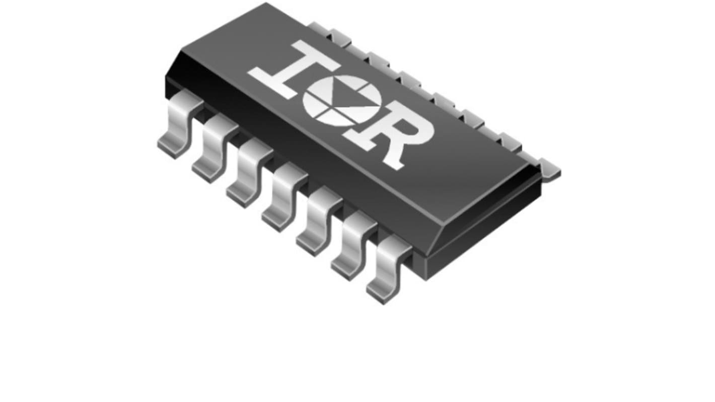
Infineon IRS21834STRPBF, Gate Driver 625 V, SOIC-14N
- RS庫存編號:
- 258-4012
- 製造零件編號:
- IRS21834STRPBF
- 製造商:
- Infineon

可享批量折扣
小計(1 包,共 2 件)*
TWD104.00
(不含稅)
TWD109.20
(含稅)
訂單超過 $1,300.00 免費送貨
有庫存
- 4,992 件準備從其他地點送貨
**需要更多嗎?**輸入您需要的數量,然後按一下「查看送貨日期」以查詢更多庫存和送貨詳細資訊。
單位 | 每單位 | 每包* |
|---|---|---|
| 2 - 8 | TWD52.00 | TWD104.00 |
| 10 - 98 | TWD46.50 | TWD93.00 |
| 100 - 248 | TWD44.00 | TWD88.00 |
| 250 - 498 | TWD38.00 | TWD76.00 |
| 500 + | TWD37.00 | TWD74.00 |
* 參考價格
- RS庫存編號:
- 258-4012
- 製造零件編號:
- IRS21834STRPBF
- 製造商:
- Infineon
規格
產品概覽和技術數據資料表
法例與合規
產品詳細資訊
透過選取一個或多個屬性來查找類似產品。
選取全部 | 屬性 | 值 |
|---|---|---|
| 品牌 | Infineon | |
| Product Type | Gate Driver Module | |
| Package Type | SOIC-14N | |
| Fall Time | 35ns | |
| Driver Type | Gate Driver | |
| Rise Time | 40ns | |
| Minimum Supply Voltage | 3.3V | |
| Maximum Supply Voltage | 625V | |
| Minimum Operating Temperature | -40°C | |
| Maximum Operating Temperature | 125°C | |
| Standards/Approvals | No | |
| Automotive Standard | No | |
| 選取全部 | ||
|---|---|---|
品牌 Infineon | ||
Product Type Gate Driver Module | ||
Package Type SOIC-14N | ||
Fall Time 35ns | ||
Driver Type Gate Driver | ||
Rise Time 40ns | ||
Minimum Supply Voltage 3.3V | ||
Maximum Supply Voltage 625V | ||
Minimum Operating Temperature -40°C | ||
Maximum Operating Temperature 125°C | ||
Standards/Approvals No | ||
Automotive Standard No | ||
The Infineon half bridge driver are high voltage, high speed power MOSFET and IGBT drivers with dependent high-side and low-side referenced output channels. Proprietary HVIC and latch immune CMOS technologies enable ruggedized monolithic construction. The logic input is compatible with standard CMOS or LSTTL output, down to 3.3 V logic. The output drivers feature a high pulse current buffer stage designed for minimum driver cross-conduction. The floating channel can be used to drive an N-channel power MOSFET or IGBT in the high-side configuration which operates up to 600 V.
Gate drive supply range from 10 V to 20 V
Under voltage lockout for both channels
3.3 V and 5 V input logic compatible
Matched propagation delay for both channels
Logic and power ground +/- 5 V offset
Lower di/dt gate driver for better noise immunity
Output source/sink current capability 1.4 A/1.8 A
RoHS compliant
