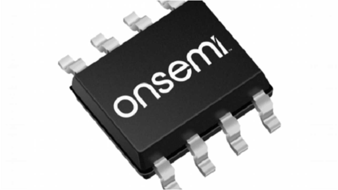
onsemi MOSFET Gate Driver, 6.5 A 8-Pin 22 V, SOIC
- RS庫存編號:
- 244-9170
- 製造零件編號:
- NCV57091BDWR2G
- 製造商:
- onsemi

此圖片僅供參考,請參閲產品詳細資訊及規格
暫時無法供應
我們無法確定此產品何時有貨,RS 預計將其從我們的產品目錄中移除。
- RS庫存編號:
- 244-9170
- 製造零件編號:
- NCV57091BDWR2G
- 製造商:
- onsemi
規格
產品概覽和技術數據資料表
法例與合規
產品詳細資訊
透過選取一個或多個屬性來查找類似產品。
選取全部 | 屬性 | 值 |
|---|---|---|
| 品牌 | onsemi | |
| Product Type | MOSFET | |
| Output Current | 6.5A | |
| Pin Count | 8 | |
| Fall Time | 13ns | |
| Package Type | SOIC | |
| Driver Type | MOSFET | |
| Rise Time | 30ns | |
| Minimum Supply Voltage | 22V | |
| Maximum Supply Voltage | 22V | |
| Minimum Operating Temperature | -40°C | |
| Maximum Operating Temperature | 150°C | |
| Series | NCV57 | |
| Standards/Approvals | No | |
| Mount Type | PCB | |
| Automotive Standard | No | |
| 選取全部 | ||
|---|---|---|
品牌 onsemi | ||
Product Type MOSFET | ||
Output Current 6.5A | ||
Pin Count 8 | ||
Fall Time 13ns | ||
Package Type SOIC | ||
Driver Type MOSFET | ||
Rise Time 30ns | ||
Minimum Supply Voltage 22V | ||
Maximum Supply Voltage 22V | ||
Minimum Operating Temperature -40°C | ||
Maximum Operating Temperature 150°C | ||
Series NCV57 | ||
Standards/Approvals No | ||
Mount Type PCB | ||
Automotive Standard No | ||
The ON Semiconductor Gate Driver are isolated dual−channel gate drivers with 4.5−A/9−A source and sink peak current respectively. They are designed for fast switching to drive power MOSFETs, and SiC MOSFET power switches. The NCP51561 offers short and matched propagation delays. Two independent and 5 kVrms internal galvanic isolation from input to each output and internal functional isolation between the two output drivers allows a working voltage of up to 1500 VDC. This driver can be used in any possible configurations of two low side, two high−side switches or a half−bridge driver with programmable dead time. An ENA/DIS pin shutdowns both outputs simultaneously when set low or high for ENABLE or DISABLE mode respectively. The NCP51561 offers other important protection functions such as independent under−voltage lockout for both gate drivers and a Dead Time adjustment function.
4.5 A Peak Source, 9 A Peak Sink Output Current Capability
Flexible: Dual Low−Side, Dual High−Side or Half−Bridge Gate Driver
Independent UVLO Protections for Both Output Drivers
Output Supply Voltage from 6.5 V to 30 V with 5−V and 8−V for MOSFET, 13−V and 17−V UVLO for SiC, Thresholds.
Common Mode Transient Immunity CMTI > 200 V/ns
Propagation Delay Typical 36 ns with 5 ns Max Delay Matching per Channel and 5 ns Max Pulse−Width Distortion
User Programmable Input Logic Single or Dual−Input Modes via ANB and ENABLE or DISABLE Mode
User Programmable Dead−Time
相關連結
- onsemi NCV57091BDWR2G MOSFET Gate Driver SOIC
- onsemi MOSFET Gate Driver SOIC
- onsemi NCV57091ADWR2G MOSFET Gate Driver SOIC
- onsemi MOSFET Gate Driver SOIC
- onsemi NCD57091ADWR2G MOSFET Gate Driver SOIC
- onsemi NCD57091BDWR2G MOSFET Gate Driver SOIC
- onsemi NCD57091CDWR2G MOSFET Gate Driver SOIC
- onsemi NCV57091CDWR2G MOSFET Gate Driver SOIC
