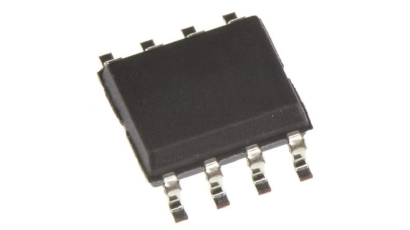
onsemi NCD57090EDWR2G, IGBT, 6.5 A 8-Pin 20 V, SOIC
- RS庫存編號:
- 230-9048
- 製造零件編號:
- NCD57090EDWR2G
- 製造商:
- onsemi

此圖片僅供參考,請參閲產品詳細資訊及規格
暫時無法供應
我們無法確定此產品何時有貨,RS 預計將其從我們的產品目錄中移除。
- RS庫存編號:
- 230-9048
- 製造零件編號:
- NCD57090EDWR2G
- 製造商:
- onsemi
規格
產品概覽和技術數據資料表
法例與合規
產品詳細資訊
透過選取一個或多個屬性來查找類似產品。
選取全部 | 屬性 | 值 |
|---|---|---|
| 品牌 | onsemi | |
| Product Type | IGBT Module | |
| Output Current | 6.5A | |
| Pin Count | 8 | |
| Fall Time | 13ns | |
| Package Type | SOIC | |
| Number of Outputs | 5 | |
| Driver Type | IGBT | |
| Rise Time | 13ns | |
| Minimum Supply Voltage | 20V | |
| Maximum Supply Voltage | 20V | |
| Minimum Operating Temperature | -40°C | |
| Maximum Operating Temperature | 125°C | |
| Height | 1.75mm | |
| Series | NCD57090 | |
| Standards/Approvals | No | |
| Length | 5mm | |
| Width | 4 mm | |
| Mount Type | Surface | |
| Automotive Standard | AEC-Q100 | |
| 選取全部 | ||
|---|---|---|
品牌 onsemi | ||
Product Type IGBT Module | ||
Output Current 6.5A | ||
Pin Count 8 | ||
Fall Time 13ns | ||
Package Type SOIC | ||
Number of Outputs 5 | ||
Driver Type IGBT | ||
Rise Time 13ns | ||
Minimum Supply Voltage 20V | ||
Maximum Supply Voltage 20V | ||
Minimum Operating Temperature -40°C | ||
Maximum Operating Temperature 125°C | ||
Height 1.75mm | ||
Series NCD57090 | ||
Standards/Approvals No | ||
Length 5mm | ||
Width 4 mm | ||
Mount Type Surface | ||
Automotive Standard AEC-Q100 | ||
The ON Semiconductor series NCD57090E are high−current single channel IGBT gate drivers with 5 kVrms internal galvanic isolation, designed for high system efficiency and reliability in high power applications. The devices accept complementary inputs and depending on the pin configuration, offer options such as Active Miller Clamp (NCD57090E). NCD57090E accommodate wide range of input bias voltage and signal levels from 3.3 V to 20 V.
Improves system efficiency
Short Propagation Delays with Accurate Matching
Improves PWM signal integrity
High Transient & Electromagnetic Immunity
Ruggedness in fast slew rate high voltage and high current switching applications
5 KVrms On-Chip Galvanic Isolation
Saves cost and board space while offering improved performance compared to opto-drivers
Wide Bias Voltage Ranges and Input Voltage Range
Offers system design flexibility and allows the usage of commonly available system voltage rails
Active Miller Clamp or Negative Gate Voltage or Split Outputs
Offers a choice in selecting the right feature in a compact package
