Lattice FPGA iCE40 LP/HX 1280 Cells, 64 kB 160 Blocks, 49-Pin UCBGA
- RS庫存編號:
- 168-4224
- 製造零件編號:
- ICE40LP1K-CM49
- 製造商:
- Lattice Semiconductor

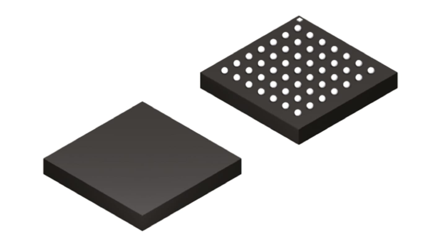
此圖片僅供參考,請參閲產品詳細資訊及規格
暫時無法供應
我們無法確定此產品何時有貨,RS 預計將其從我們的產品目錄中移除。
- RS庫存編號:
- 168-4224
- 製造零件編號:
- ICE40LP1K-CM49
- 製造商:
- Lattice Semiconductor
規格
產品概覽和技術數據資料表
法例與合規
產品詳細資訊
透過選取一個或多個屬性來查找類似產品。
選取全部 | 屬性 | 值 |
|---|---|---|
| 品牌 | Lattice Semiconductor | |
| Series | iCE40 LP/HX | |
| Product Type | FPGA | |
| Number of Logic Cells | 1280 | |
| Number of Logic Units | 160 | |
| Number of Registers | 1280 | |
| Mount Type | Surface | |
| Minimum Supply Voltage | 1.14V | |
| Package Type | UCBGA | |
| Pin Count | 49 | |
| Maximum Supply Voltage | 1.26V | |
| Minimum Operating Temperature | -40°C | |
| Number of RAM Bits | 64kB | |
| Maximum Operating Temperature | 85°C | |
| Height | 0.9mm | |
| Length | 3mm | |
| Standards/Approvals | Halogen Free | |
| Automotive Standard | No | |
| 選取全部 | ||
|---|---|---|
品牌 Lattice Semiconductor | ||
Series iCE40 LP/HX | ||
Product Type FPGA | ||
Number of Logic Cells 1280 | ||
Number of Logic Units 160 | ||
Number of Registers 1280 | ||
Mount Type Surface | ||
Minimum Supply Voltage 1.14V | ||
Package Type UCBGA | ||
Pin Count 49 | ||
Maximum Supply Voltage 1.26V | ||
Minimum Operating Temperature -40°C | ||
Number of RAM Bits 64kB | ||
Maximum Operating Temperature 85°C | ||
Height 0.9mm | ||
Length 3mm | ||
Standards/Approvals Halogen Free | ||
Automotive Standard No | ||
- COO (Country of Origin):
- KR
Field Programmable Gate Arrays, Lattice Semiconductor
An FPGA is a semiconductor device consisting of a Matrix of Configurable Logic Blocks (CLBs) connected through programmable interconnects. The user determines these interconnections by programming SRAM. A CLB can be simple (AND, OR gates, etc) or complex (a Block of RAM). The FPGA allows changes to be MADE to a design even after the device is soldered into a PCB.