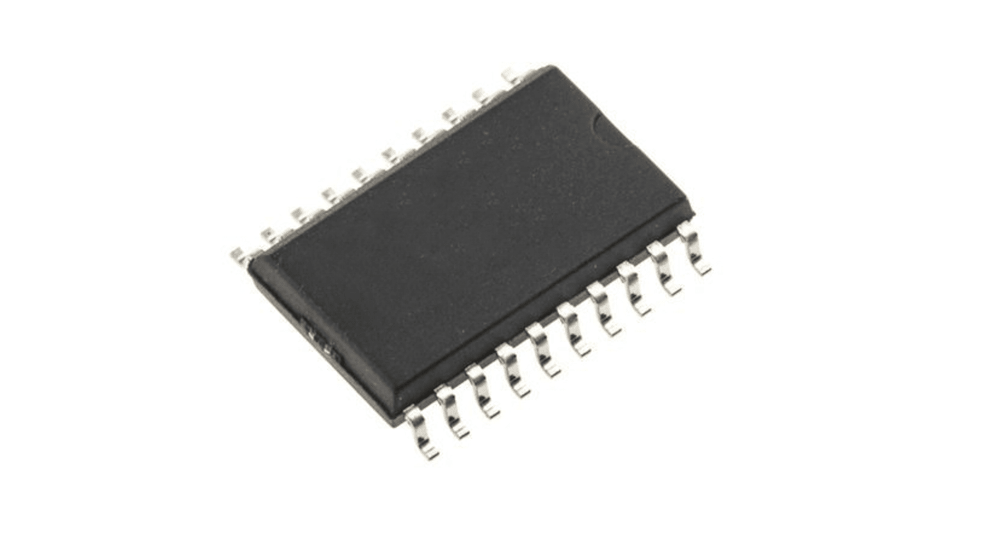
Renesas Electronics 49FCT3805DQGI Clock Driver, 20-Pin 10 SOIC
- RS庫存編號:
- 254-4927
- 製造零件編號:
- 49FCT3805DQGI
- 製造商:
- Renesas Electronics

可享批量折扣
查看批量定價選項小計(1 包,共 5 件)*
TWD452.00
(不含稅)
TWD474.60
(含稅)
訂單超過 $1,300.00 免費送貨
正在逐步停售
- 最終 260 個,準備發貨
單位 | 每單位 | 每包* |
|---|---|---|
| 5 - 5 | TWD90.40 | TWD452.00 |
| 10 - 20 | TWD81.40 | TWD407.00 |
| 25 - 105 | TWD77.20 | TWD386.00 |
| 110 - 270 | TWD75.60 | TWD378.00 |
| 275 + | TWD73.80 | TWD369.00 |
* 參考價格
- RS庫存編號:
- 254-4927
- 製造零件編號:
- 49FCT3805DQGI
- 製造商:
- Renesas Electronics
規格
產品概覽和技術數據資料表
法例與合規
產品詳細資訊
透過選取一個或多個屬性來查找類似產品。
選取全部 | 屬性 | 值 |
|---|---|---|
| 品牌 | Renesas Electronics | |
| Product Type | Clock Driver | |
| Mount Type | Surface | |
| Package Type | SOIC | |
| Pin Count | 20 | |
| Minimum Supply Voltage | 3V | |
| Maximum Supply Voltage | 3.6V | |
| Minimum Operating Temperature | -40°C | |
| Maximum Operating Temperature | 85°C | |
| Standards/Approvals | No | |
| Series | 49FCT | |
| Automotive Standard | No | |
| Maximum Output Frequency | 166MHz | |
| 選取全部 | ||
|---|---|---|
品牌 Renesas Electronics | ||
Product Type Clock Driver | ||
Mount Type Surface | ||
Package Type SOIC | ||
Pin Count 20 | ||
Minimum Supply Voltage 3V | ||
Maximum Supply Voltage 3.6V | ||
Minimum Operating Temperature -40°C | ||
Maximum Operating Temperature 85°C | ||
Standards/Approvals No | ||
Series 49FCT | ||
Automotive Standard No | ||
Maximum Output Frequency 166MHz | ||
The Renesas Electronics 3.3 volt clock driver built using advanced CMOS technology. The device consists of two banks of drivers, each with a 1:5 fanout and its own output enable control. The device has a heartbeat monitor fordiagnostics and PLL driving. The MON output is identical to all other outputs and complies with the output specifications in this document. It offers low capacitance inputs. It is designed for high speed clock distribution where signal quality and skew are critical. It also allows single point-to-point transmission line driving in applications such as address distribution, where one signal must be distributed to multiple recievers with low skew and high signal quality.
Advanced CMOS technology
Guaranteed low skew < 200 ps (max)
Very low propagation delay < 2.5 ns (max)
Very low duty cycle distortion < 270 ps (max)
Very low CMOS power levels
Operating frequency up to 166 MHz
TTL compatible inputs and outputs
Inputs can be driven from 3.3 V or 5 V components
Two independent output banks with 3-state control
Available in SSOP and QSOP packages
相關連結
- Renesas Electronics 49FCT3805DQGI Clock Driver, 20-Pin 10 SOIC
- Renesas Electronics 74FCT3807ASOG PLL Clock Driver, 20-Pin 10 SOIC
- Renesas Electronics 74FCT3807AQG8 Clock Driver, 20-Pin 10 QSOP
- Renesas Electronics 74FCT3807QGI8 Clock Driver, 20-Pin 10 QSOP
- Renesas Electronics 74FCT3807APYGI8 Clock Driver, 20-Pin 10 SSOP
- Renesas Electronics 74FCT3807PYG8 Clock Buffer, 20-Pin 10 SOIC
- Renesas Electronics 74FCT3807ASOG8 Clock Buffer, 20-Pin 10 SOIC
- Renesas Electronics 74FCT3807DPYGI PLL Clock Driver, 20-Pin 10 SSOP