Nexperia Logic Level Translator, 8-Bit Non-Inverting TTL, 24-Pin SOT-8024
- RS庫存編號:
- 243-4423
- 製造零件編號:
- 74LVC8T245BZX
- 製造商:
- Nexperia

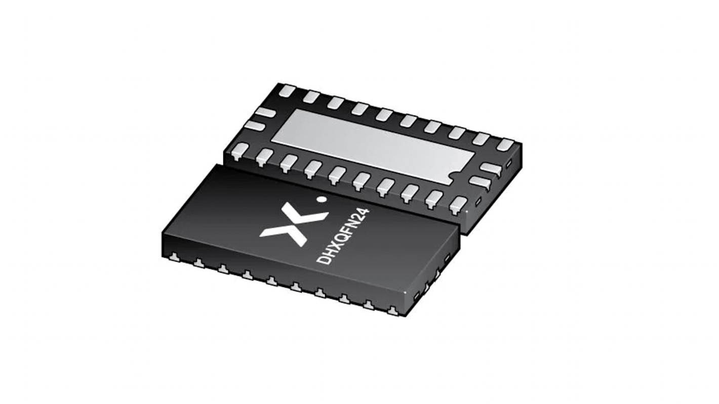
此圖片僅供參考,請參閲產品詳細資訊及規格
可享批量折扣
查看批量定價選項小計(1 卷,共 3000 件)*
TWD64,500.00
(不含稅)
TWD67,740.00
(含稅)
訂單超過 $1,300.00 免費送貨
暫時缺貨
- 從 2026年12月04日 發貨
**需要更多嗎?**輸入您需要的數量,然後按一下「查看送貨日期」以查詢更多庫存和送貨詳細資訊。
單位 | 每單位 | 每卷* |
|---|---|---|
| 3000 - 12000 | TWD21.50 | TWD64,500.00 |
| 15000 + | TWD20.80 | TWD62,400.00 |
* 參考價格
- RS庫存編號:
- 243-4423
- 製造零件編號:
- 74LVC8T245BZX
- 製造商:
- Nexperia
規格
產品概覽和技術數據資料表
法例與合規
產品詳細資訊
透過選取一個或多個屬性來查找類似產品。
選取全部 | 屬性 | 值 |
|---|---|---|
| 品牌 | Nexperia | |
| Logic Family | 74LVC | |
| Product Type | Logic Level Translator | |
| Logic Function | Translating Transceiver | |
| Number of Channels | 8 | |
| Polarity | Non-Inverting | |
| Mount Type | Surface | |
| Package Type | SOT-8024 | |
| Minimum Supply Voltage | 3V | |
| Pin Count | 24 | |
| Maximum Supply Voltage | 5.5V | |
| Input Level | TTL | |
| Output Level | TTL | |
| Maximum Propagation Delay Time @ CL | 4.1ns | |
| Minimum Operating Temperature | -40°C | |
| Maximum High Level Output Current | 24mA | |
| Maximum Operating Temperature | 125°C | |
| Height | 0.48mm | |
| Maximum Low Level Output Current | 24mA | |
| Standards/Approvals | RoHS | |
| Length | 2mm | |
| Series | 74LVC8T245 | |
| Output Type | 3 State | |
| Automotive Standard | No | |
| 選取全部 | ||
|---|---|---|
品牌 Nexperia | ||
Logic Family 74LVC | ||
Product Type Logic Level Translator | ||
Logic Function Translating Transceiver | ||
Number of Channels 8 | ||
Polarity Non-Inverting | ||
Mount Type Surface | ||
Package Type SOT-8024 | ||
Minimum Supply Voltage 3V | ||
Pin Count 24 | ||
Maximum Supply Voltage 5.5V | ||
Input Level TTL | ||
Output Level TTL | ||
Maximum Propagation Delay Time @ CL 4.1ns | ||
Minimum Operating Temperature -40°C | ||
Maximum High Level Output Current 24mA | ||
Maximum Operating Temperature 125°C | ||
Height 0.48mm | ||
Maximum Low Level Output Current 24mA | ||
Standards/Approvals RoHS | ||
Length 2mm | ||
Series 74LVC8T245 | ||
Output Type 3 State | ||
Automotive Standard No | ||
The Nexperia 8-bit dual supply translating transceivers with 3-state outputs that enable bidirectional level translation. They feature two data input-output ports (pins An and Bn), a direction control input (DIR), an output enable input (OE) and dual supply pins (VCC(A) and VCC(B)). Both VCC(A) and VCC(B) can be supplied at any voltage between 1.2 V and 5.5 V making the device suitable for translating between any of the low voltage nodes (1.2 V, 1.5 V, 1.8 V, 2.5 V, 3.3 V and 5.0 V). Pins An, OE and DIR are referenced to VCC(A) and pins Bn are referenced to VCC(B). A HIGH on DIR allows transmission from An to Bn and a LOW on DIR allows transmission from Bn to An.
Suspend mode
Latch-up performance exceeds 100 mA per JESD 78B Class II
±24 mA output drive (VCC = 3.0 V)
Inputs accept voltages up to 5.5 V
Low power consumption 30 μA maximum ICC
IOFF circuitry provides partial Power-down mode operation
Specified from -40 °C to +85 °C and -40 °C to +125 °C
The output enable input (OE) can be used to disable the outputs so the buses are effectively isolated. The devices are fully specified for partial power-down applications using IOFF. The IOFF circuitry disables the output, preventing any damaging backflow current through the device when it is powered down. In suspend mode when either VCC(A) or VCC(B) are at GND level, both A port and B port are in the high-impedance OFF-state. Active bus hold circuitry in the 74LVCH8T245 holds unused or floating data inputs at a valid logic level.
相關連結
- Nexperia 74LVC8T245BZX Logic Level Translator 24-Pin SOT-8024
- Nexperia Bus Transceiver Non-Inverting TTL, 20-Pin TSSOP
- Nexperia 74HC245PW 20-Pin TSSOP
- Nexperia Bus Transceiver 48-Pin TSSOP
- Nexperia Bus Transceiver 20-Pin SOT-8020
- Nexperia Bus Transceiver TTL, 20-Pin DHVQFN
- Nexperia 74LVT16245BDGG 16-Bit Non-Inverting TTL, 48-Pin TSSOP
- Nexperia 74HC245PW 8-Bit Non-Inverting TTL, 20-Pin TSSOP