Nexperia, 1-Channel Schmitt Trigger Input Open Drain Buffer, 8-Pin XSON
- RS庫存編號:
- 152-7175
- 製造零件編號:
- 74AXP2T3407GTX
- 製造商:
- Nexperia

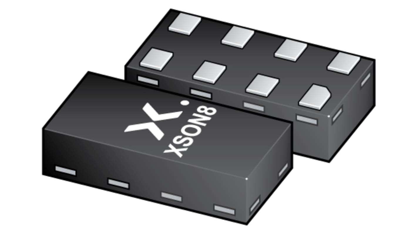
此圖片僅供參考,請參閲產品詳細資訊及規格
可享批量折扣
小計(1 卷,共 5000 件)*
TWD60,500.00
(不含稅)
TWD63,500.00
(含稅)
訂單超過 $1,300.00 免費送貨
暫時缺貨
- 從 2026年11月04日 發貨
**需要更多嗎?**輸入您需要的數量,然後按一下「查看送貨日期」以查詢更多庫存和送貨詳細資訊。
單位 | 每單位 | 每卷* |
|---|---|---|
| 5000 - 5000 | TWD12.10 | TWD60,500.00 |
| 10000 + | TWD11.80 | TWD59,000.00 |
* 參考價格
- RS庫存編號:
- 152-7175
- 製造零件編號:
- 74AXP2T3407GTX
- 製造商:
- Nexperia
規格
產品概覽和技術數據資料表
法例與合規
產品詳細資訊
透過選取一個或多個屬性來查找類似產品。
選取全部 | 屬性 | 值 |
|---|---|---|
| 品牌 | Nexperia | |
| Logic Family | AXP | |
| Product Type | Buffer | |
| Logic Function | Single Buffer | |
| Number of Channels | 1 | |
| Schmitt Trigger Input | Yes | |
| Input Type | Open Drain | |
| Output Type | Open Drain | |
| Mount Type | Surface | |
| Minimum Supply Voltage | 0.7V | |
| Package Type | XSON | |
| Pin Count | 8 | |
| Maximum Supply Voltage | 2.75V | |
| Minimum Operating Temperature | -40°C | |
| Maximum Propagation Delay Time @ CL | 72ns | |
| Maximum Operating Temperature | 85°C | |
| Height | 0.496mm | |
| Length | 2mm | |
| Standards/Approvals | RoHS | |
| Series | 74AXP2T3407 | |
| Supply Current | 50mA | |
| Automotive Standard | No | |
| 選取全部 | ||
|---|---|---|
品牌 Nexperia | ||
Logic Family AXP | ||
Product Type Buffer | ||
Logic Function Single Buffer | ||
Number of Channels 1 | ||
Schmitt Trigger Input Yes | ||
Input Type Open Drain | ||
Output Type Open Drain | ||
Mount Type Surface | ||
Minimum Supply Voltage 0.7V | ||
Package Type XSON | ||
Pin Count 8 | ||
Maximum Supply Voltage 2.75V | ||
Minimum Operating Temperature -40°C | ||
Maximum Propagation Delay Time @ CL 72ns | ||
Maximum Operating Temperature 85°C | ||
Height 0.496mm | ||
Length 2mm | ||
Standards/Approvals RoHS | ||
Series 74AXP2T3407 | ||
Supply Current 50mA | ||
Automotive Standard No | ||
Dual supply single buffer and single buffer with open-drain, The 74AXP2T3407 is a dual supply single buffer and a single buffer with open-drain output. It features two input pins (nA), an output pin (1Y) and an open-drain output pin (2Y) and dual supply pins (VCCI and VCCO). The inputs are referenced to VCCI and the output is referenced to VCCO. All inputs can be connected directly to VCCI or GND. VCCI can be supplied at any voltage between 0.7 V and 2.75 V and VCCO can be supplied at any voltage between 1.2 V and 5.5 V.
High noise immunity
Inputs accept voltages up to 2.75 V
Low noise overshoot and undershoot < 10% of VCCO
IOFF circuitry provides partial power-down mode operation