Power Integrations, Link Switch 575 A 8-Pin, SO-8C LNK3307D-TL
- RS庫存編號:
- 228-6367
- 製造零件編號:
- LNK3307D-TL
- 製造商:
- Power Integrations

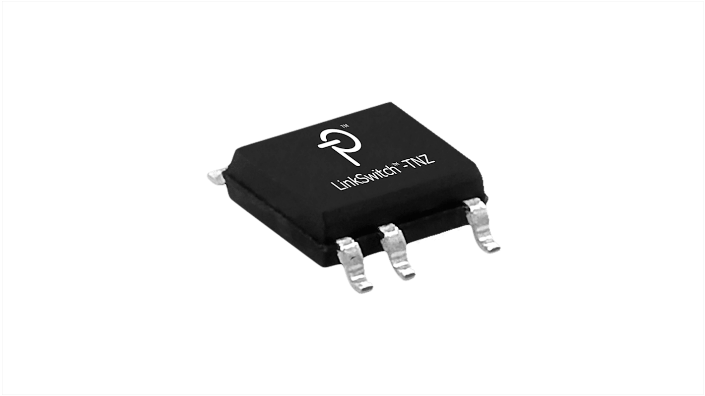
此圖片僅供參考,請參閲產品詳細資訊及規格
可享批量折扣
小計(1 包,共 5 件)*
TWD171.00
(不含稅)
TWD179.55
(含稅)
訂單超過 $1,300.00 免費送貨
有庫存
- 2,270 件準備從其他地點送貨
**需要更多嗎?**輸入您需要的數量,然後按一下「查看送貨日期」以查詢更多庫存和送貨詳細資訊。
單位 | 每單位 | 每包* |
|---|---|---|
| 5 - 5 | TWD34.20 | TWD171.00 |
| 10 - 95 | TWD33.60 | TWD168.00 |
| 100 - 245 | TWD32.80 | TWD164.00 |
| 250 - 495 | TWD32.20 | TWD161.00 |
| 500 + | TWD31.60 | TWD158.00 |
* 參考價格
- RS庫存編號:
- 228-6367
- 製造零件編號:
- LNK3307D-TL
- 製造商:
- Power Integrations
規格
產品概覽和技術數據資料表
法例與合規
產品詳細資訊
透過選取一個或多個屬性來查找類似產品。
選取全部 | 屬性 | 值 |
|---|---|---|
| 品牌 | Power Integrations | |
| Maximum Input Voltage | 70V | |
| Product Type | Link Switch | |
| Mount Type | Surface | |
| Output Power | 10W | |
| Switching Frequency | 66kHz | |
| Pin Count | 8 | |
| Maximum Output Current | 575A | |
| Package Type | SO-8C | |
| Minimum Input Voltage | 85V | |
| Topology | Flyback | |
| Minimum Operating Temperature | -40°C | |
| Maximum Duty Cycle | 0.69% | |
| Maximum Operating Temperature | 150°C | |
| Length | 4.9mm | |
| Series | LinkSwitch-TNZ | |
| Standards/Approvals | RoHS | |
| Height | 6mm | |
| Automotive Standard | No | |
| Supply Current | 180μA | |
| Minimum Output Current | 120mA | |
| 選取全部 | ||
|---|---|---|
品牌 Power Integrations | ||
Maximum Input Voltage 70V | ||
Product Type Link Switch | ||
Mount Type Surface | ||
Output Power 10W | ||
Switching Frequency 66kHz | ||
Pin Count 8 | ||
Maximum Output Current 575A | ||
Package Type SO-8C | ||
Minimum Input Voltage 85V | ||
Topology Flyback | ||
Minimum Operating Temperature -40°C | ||
Maximum Duty Cycle 0.69% | ||
Maximum Operating Temperature 150°C | ||
Length 4.9mm | ||
Series LinkSwitch-TNZ | ||
Standards/Approvals RoHS | ||
Height 6mm | ||
Automotive Standard No | ||
Supply Current 180μA | ||
Minimum Output Current 120mA | ||
The Power Integration LinkSwitch-TNZ series of ICs combine power conversion with lossless generation of AC zero crossing signal used typically for system clock and timing functions. Each device incorporates a 725 V power MOSFET, oscillator, a high-voltage switched current source for self-biasing, frequency jittering, fast current limit, hysteretic thermal shutdown, and output and input overvoltage protection circuitry onto a monolithic IC.
Lossless zero cross signal generation
Supports buck, buck-boost and flyback topologies
Frequency jittering reduces EMI filter complexity
Soft-start limits system component stress at start-up
Hysteretic over-temperature protection