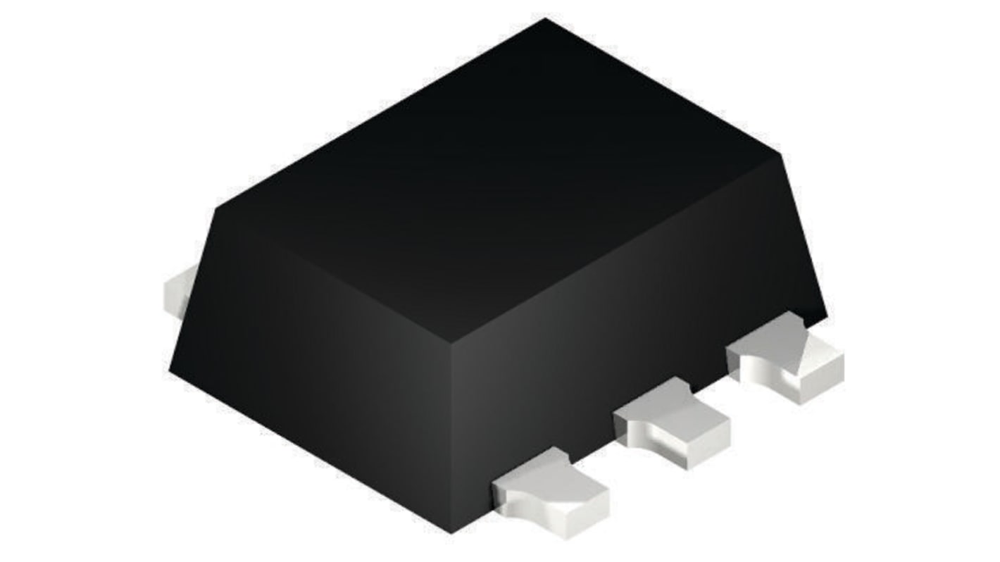
Dual N-Channel MOSFET, 600 mA, 20 V, 6-Pin SC-89-6 onsemi FDY3000NZ

- RS庫存編號:
- 166-1809
- 製造零件編號:
- FDY3000NZ
- 製造商:
- onsemi
18000 現貨庫存,可於6工作日發貨。
已增加
單價(不含稅) 個 (在毎卷:3000)
TWD4.50
(不含稅)
TWD4.72
(含稅)
| 單位 | Per unit | Per Reel* |
| 3000 - 12000 | TWD4.50 | TWD13,500.00 |
| 15000 + | TWD4.30 | TWD12,900.00 |
| * 參考價格 | ||
- RS庫存編號:
- 166-1809
- 製造零件編號:
- FDY3000NZ
- 製造商:
- onsemi
法例與合規
產品詳細資訊
PowerTrench® Dual N-Channel MOSFET, Fairchild Semiconductor
ON Semis PowerTrench® MOSFETS are optimised power switched that offer increased system efficiency and power density. They combine small gate charge, small reverse recovery and a soft reverse recovery body diode to contribute to fast switching of synchronous rectification in AC/DC power supplies.
The soft body diode performance of the PowerTrench® MOSFETs is able to eliminate snubber circuit or replace a higher voltage rating MOSFET.
The soft body diode performance of the PowerTrench® MOSFETs is able to eliminate snubber circuit or replace a higher voltage rating MOSFET.
For products that are Customized and under Non-cancellable & Non-returnable, Sales & Conditions apply.
MOSFET Transistors, ON Semi
ON Semi offers a substantial portfolio of MOSFET devices that includes high-voltage (>250V) and low-voltage (<250V) types. The advanced silicon technology provides smaller die sizes, which it is incorporated into multiple industry-standard and thermally-enhanced packages.
ON Semi MOSFETs provide superior design reliability from reduced voltage spikes and overshoot, to lower junction capacitance and reverse recovery charge, to elimination of additional external components to keep systems up and running longer.
ON Semi MOSFETs provide superior design reliability from reduced voltage spikes and overshoot, to lower junction capacitance and reverse recovery charge, to elimination of additional external components to keep systems up and running longer.
規格
屬性 | 值 |
|---|---|
| Channel Type | N |
| Maximum Continuous Drain Current | 600 mA |
| Maximum Drain Source Voltage | 20 V |
| Series | PowerTrench |
| Package Type | SC-89-6 |
| Mounting Type | Surface Mount |
| Pin Count | 6 |
| Maximum Drain Source Resistance | 700 mΩ |
| Channel Mode | Enhancement |
| Minimum Gate Threshold Voltage | 0.6V |
| Maximum Power Dissipation | 625 mW |
| Transistor Configuration | Isolated |
| Maximum Gate Source Voltage | -12 V, +12 V |
| Transistor Material | Si |
| Typical Gate Charge @ Vgs | 0.8 nC @ 4.5 V |
| Maximum Operating Temperature | +150 °C |
| Length | 1.6mm |
| Number of Elements per Chip | 2 |
| Width | 1.2mm |
| Minimum Operating Temperature | -55 °C |
| Height | 0.5mm |